data communications application note dan183 - Digi
advertisement
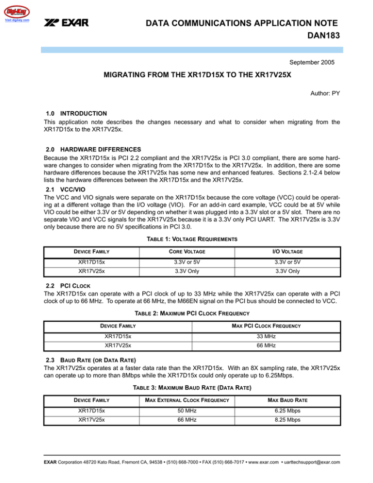
xr DATA COMMUNICATIONS APPLICATION NOTE DAN183 September 2005 MIGRATING FROM THE XR17D15X TO THE XR17V25X Author: PY 1.0 INTRODUCTION This application note describes the changes necessary and what to consider when migrating from the XR17D15x to the XR17V25x. 2.0 HARDWARE DIFFERENCES Because the XR17D15x is PCI 2.2 compliant and the XR17V25x is PCI 3.0 compliant, there are some hardware changes to consider when migrating from the XR17D15x to the XR17V25x. In addition, there are some hardware differences because the XR17V25x has some new and enhanced features. Sections 2.1-2.4 below lists the hardware differences between the XR17D15x and the XR17V25x. 2.1 VCC/VIO The VCC and VIO signals were separate on the XR17D15x because the core voltage (VCC) could be operating at a different voltage than the I/O voltage (VIO). For an add-in card example, VCC could be at 5V while VIO could be either 3.3V or 5V depending on whether it was plugged into a 3.3V slot or a 5V slot. There are no separate VIO and VCC signals for the XR17V25x because it is a 3.3V only PCI UART. The XR17V25x is 3.3V only because there are no 5V specifications in PCI 3.0. TABLE 1: VOLTAGE REQUIREMENTS DEVICE FAMILY CORE VOLTAGE I/O VOLTAGE XR17D15x 3.3V or 5V 3.3V or 5V XR17V25x 3.3V Only 3.3V Only 2.2 PCI CLOCK The XR17D15x can operate with a PCI clock of up to 33 MHz while the XR17V25x can operate with a PCI clock of up to 66 MHz. To operate at 66 MHz, the M66EN signal on the PCI bus should be connected to VCC. TABLE 2: MAXIMUM PCI CLOCK FREQUENCY DEVICE FAMILY MAX PCI CLOCK FREQUENCY XR17D15x 33 MHz XR17V25x 66 MHz 2.3 BAUD RATE (OR DATA RATE) The XR17V25x operates at a faster data rate than the XR17D15x. With an 8X sampling rate, the XR17V25x can operate up to more than 8Mbps while the XR17D15x could only operate up to 6.25Mbps. TABLE 3: MAXIMUM BAUD RATE (DATA RATE) DEVICE FAMILY MAX EXTERNAL CLOCK FREQUENCY MAX BAUD RATE XR17D15x 50 MHz 6.25 Mbps XR17V25x 66 MHz 8.25 Mbps EXAR Corporation 48720 Kato Road, Fremont CA, 94538 • (510) 668-7000 • FAX (510) 668-7017 • www.exar.com • uarttechsupport@exar.com xr DATA COMMUNICATIONS APPLICATION NOTE DAN183 2.4 PIN DIFFERENCE The TEST# pin (input pin used for factory test mode) in the XR17D15x has been changed to the PME# pin (open-drain output pin) in the XR17V25x to support Power Management. The XR17V25x is compliant with Power Management Revision 1.1 Specifications. The XR17D15x did not have any Power Management support. If Power Management is used, then the PME# pin should be connected to the PME# signal on the PCI bus interface. Otherwise, the PME# pin should be pulled-up or left floating. 3.0 FIRMWARE DIFFERENCES The internal register set of the XR17V25x is based on the internal register set of the XR17D15x. However, there were some changes/enhancements in the XR17V25x that resulted in some changes in the internal register set. Here is a list of the changes/enhancements and how the register set was affected. 3.1 FRACTIONAL BAUD RATE GENERATOR Traditionally, the baud rate divisor is a value between 1 and 32767 (or 216 - 1) that is programmed via two 8-bit registers (DLL and DLM). With these divisors, standard baud rates such as 9600 bps or 115200 bps could be achieved by using standard clock/crystal frequencies such as 1.8432 MHz or 14.7456 MHz. Use the following formula to calculate the baud rate divisor: divisor (decimal)= (clock frequency) / (baud rate X sampling rate) By default the sampling rate is 16X the clock frequency, unless the 8X sampling rate is enabled via the 8XMODE register. For example, if the desired baud rate is 115200 bps and a 14.7456 MHz clock is used, the divisor would be 8. Using these standard clock frequencies, the standard baud rates were easily achieved. However, when non-standard clock frequencies such as 10 MHz or 24 MHz were used, some standard baud rates were not possible because the divisors are not whole numbers. Using the closest whole number divisor still resulted in data transmission errors because the baud rate deviation was greater than the deviation tolerated by the UART (see DAN108 for complete details). For example, if the desired baud rate is 115200 bps and a 10 MHz clock is used, the approximate divisor would be 5.425. The table below shows the two closest divisors and the corresponding data rate error. TABLE 4: BAUD RATE ERROR IN XR17D15X DESIRED BAUD RATE (BPS) DLM DLL DLD ACTUAL BAUD RATE % ERROR 115200 0x00 0x05 N/A 125000 8.5 115200 0x00 0x06 N/A 104167 9.6 In the XR17V25x, a DLD register was added to allow fractional divisors. The value programmed into DLD would be divided by 16 and then added to the divisor. Using the same example above, the the closest divisor would be 5 and the DLD would be 7. This would result in a divisor of 5.4375. As you can see below, the resulting baud rate would be within the baud rate deviation tolerated by the UART. . TABLE 5: BAUD RATE ERROR IN XR17V25X DESIRED BAUD RATE (BPS) DLM DLL DLD ACTUAL BAUD RATE % ERROR 115200 0x00 0x05 0x07 114953 0.2 The addition of the DLD register allows more flexibility in the clock frequency that can be used with the XR17V25x to generate almost any desired baud rate. Also, if the system has a clock available, the XR17V25x can use that instead of a separate crystal. 2 DATA COMMUNICATIONS APPLICATION NOTE DAN183 xr 3.2 DEVICE ID To distinguish between the two families and their capabilities, the Device ID for the XR17V25x family is different. The upper nibble of the Device ID distinguishes between the two families. The lower nibble indicates how many UART channels there are on the device. The table below lists the Device IDs. TABLE 6: DEVICE IDS DEVICE DEVICE ID DEVICE DEVICE ID XR17D152 0x22 XR17V252 0x42 XR17D154 0x24 XR17V254 0x44 XR17D158 0x28 XR17V258 0x48 In the Windows drivers provided by Exar, the driver does check for the Device ID. When migrating from the XR17D15x to the XR17V25x, the software driver should be updated to detect the new Device IDs. Otherwise, the drivers will not install properly. 3.3 POWER MANAGEMENT Power Management registers were added at address offsets 0x40 and 0x44 in the PCI Local Bus Configuration space to support the Power Management feature in the XR17V25x. See the XR17V25x datasheet for complete details. This feature was not available in the XR17D15x. 3.4 EEPROM ADDRESS DEFINITIONS The XR17D15x only expects to read four 16-bit values from the EEPROM. However, the XR17V25x expects to read eight 16-bit values from the EEPROM. Therefore, the EEPROM should be updated so that there are 8 16-bit values programmed into the EEPROM instead of 4. The table below lists the 16-bit values that the XR17D15x and XR17V25x UARTs expect. TABLE 7: 16-BIT EEPROM DATA EEPROM MEMORY ADDRESS XR17D15X XR17V25X 0x00 Vendor ID Vendor ID 0x01 Device ID Device ID 0x02 Subsystem Vendor ID Class Code 0x03 Subsystem Device ID Class Code (continued) 0x04 - Subsystem Vendor ID 0x05 - Subsystem Device ID 0x06 - Special Register (Lower Word) 0x07 - Special Register (Upper Word) There is an EEPROM programming utility available from Exar that can program the EEPROM through the UART for the Windows 2000 or Windows XP operating system. However, to program the EEPROM through the UART, the Windows 2000/XP driver must first be installed. This driver is available to Exar customers after a Software License Agreement (SLA) has been completed. The Windows drivers and EEPROM programming utility can be obtained by sending an e-mail to uarttechsupport@exar.com. 3.5 TIMER/COUNTER In the XR17D15x, each of the first 6 bits of the TIMERCNTL register had a function. However, the Timer/ Counter functions were enhanced in the XR17V25x. In order to prevent simple errors of not masking the correct bits, the TIMERCNTL register is now command driven. A 4-bit command is used instead of each individu- 3 xr DATA COMMUNICATIONS APPLICATION NOTE DAN183 al bit. The table below lists the different Timer/Counter functions and how they are controlled in the XR17D15x and the XR17V25x. For a detailed description of the Timer/Counter, see the XR17V25x datasheet. TABLE 8: TIMER/COUNTER FUNCTIONS TIMER/COUNTER FUNCTION XR17D15X (BIT DRIVEN) XR17V25X (COMMAND DRIVEN) Disable Timer/Counter Interrupt TIMERCNTL[0] = 0 TIMERCNTL[3:0] = 0010 Enable Timer/Counter Interrupt TIMERCNTL[0] = 1 TIMERCNTL[3:0] = 0001 Stop or Pause Timer/Counter TIMERCNTL[1] = 0 TIMERCNTL[3:0] = 1010 Start Timer/Counter TIMERCNTL[1] = 1 TIMERCNTL[3:0] = 1001 Select Re-Triggerable Mode TIMERCNTL[2] = 0 TIMERCNTL[3:0] = 0100 Select One-Shot Mode TIMERCNTL[2] = 1 TIMERCNTL[3:0] = 0011 Select Internal Crystal Oscillator as clock source for the Timer/Counter TIMERCNTL[3] = 0 TIMERCNTL[3:0] = 0101 Select External Clock (via TMRCK input pin) as clock source for the Timer/Counter TIMERCNTL[3] = 1 TIMERCNTL[3:0] = 0110 De-Route Timer output from MPIO[0] pin TIMERCNTL[4] = 0 TIMERCNTL[3:0] = 1000 Route Timer output to MPIO[0] pin TIMERCNTL[4 = 1 TIMERCNTL[3:0] = 0111 - TIMERCNTL[3:0] = 1011 Reset Timer 3.6 TRANSMITTER AND RECEIVER DISABLE The Transmitter and Receive can be disabled in the XR17V25x. This feature is not available in the XR17D15x. The Transmitter is disabled when MSR bit-3 = 1 (write-only). When the Transmitter is disabled, any data left or written into the TX FIFO will not be transmitted. It will resume transmission when MSR bit-3 has been reset. Similarly, the Receiver is disabled when MSR bit-2 = 1 (write-only). When the Receiver is disabled, it will ignore any data received during that time at the RX pin. It will receive data normally when MSR bit-2 has been reset. See the XR17V25x datasheet for complete details. 3.7 TXCHAR IMMEDIATE TXCHAR Immediate is another new feature in the XR17V25x. One byte of data can be inserted into the Transmit Shift Register, ahead of any data that is remaining in the TX FIFO, after the current byte has shifted out. This is done by writing to MCR bit-3 (assuming EFR bit-4 = 1) and then writing to the THR register. This feature can only be used when the Transmitter has not been disabled. See the XR17V25x datasheet for complete details. 3.8 TX XON/XOFF INDICATOR In the XR17D15x, the XCHAR register would indicate which flow control character (XON or XOFF) was received last by a particular channel. If bit-0 = 1, then the last flow control character received was an XOFF. If bit-1 = 1, then the last flow control character received was an XON. In addition to that, the XR17V25x has 2 additional bits to indicate whether the last flow control character transmitted was an XON or XOFF character. If XCHAR bit-2 = 1, then the last flow control character transmitted was an XOFF character. If XCHAR bit-3 = 1, then the last flow control character transmitted was an XON character. 4.0 CONCLUSION The XR17V25x is an enhanced version of the XR17D15x with a faster PCI bus clock, higher data rate, and many new features. Because of these reasons, some hardware and software changes will be required to take advantage of the performance of the 66MHz PCI clock and the other enhanced features of the XR17V25x. 4 xr NOTICE EXAR Corporation reserves the right to make changes to the products contained in this publication in order to improve design, performance or reliability. EXAR Corporation assumes no responsibility for the use of any circuits described herein, conveys no license under any patent or other right, and makes no representation that the circuits are free of patent infringement. Charts and schedules contained here in are only for illustration purposes and may vary depending upon a user’s specific application. While the information in this publication has been carefully checked; no responsibility, however, is assumed for inaccuracies. EXAR Corporation does not recommend the use of any of its products in life support applications where the failure or malfunction of the product can reasonably be expected to cause failure of the life support system or to significantly affect its safety or effectiveness. Products are not authorized for use in such applications unless EXAR Corporation receives, in writing, assurances to its satisfaction that: (a) the risk of injury or damage has been minimized; (b) the user assumes all such risks; (c) potential liability of EXAR Corporation is adequately protected under the circumstances. Copyright 2005 EXAR Corporation September 2005 Send your UART technical inquiry with technical details to hotline: uarttechsupport@exar.com Reproduction, in part or whole, without the prior written consent of EXAR Corporation is prohibited. 5
