IL510/IL511/IL514/IL515/IL516
DC-Correct Digital Isolators
Features
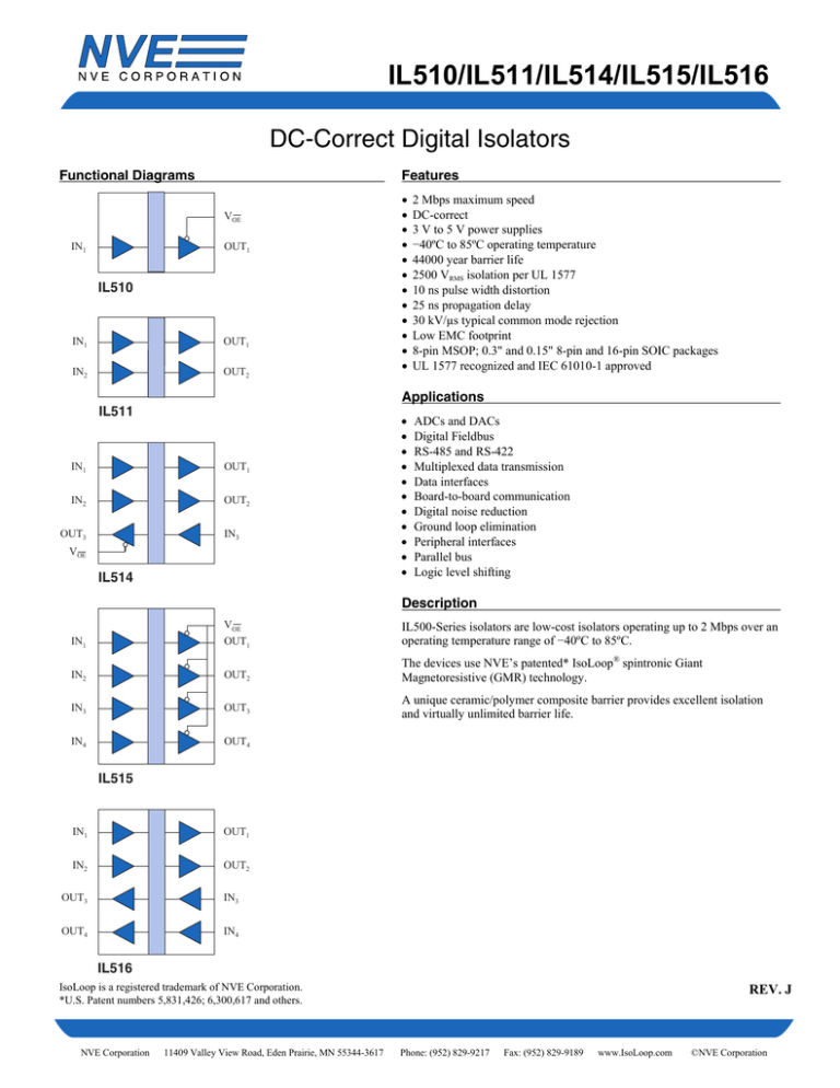
Functional Diagrams
VOE
IN1
OUT1
IL510
IN1
OUT1
IN2
OUT2
•
•
•
•
•
•
•
•
•
•
•
•
2 Mbps maximum speed
DC-correct
3 V to 5 V power supplies
−40ºC to 85ºC operating temperature
44000 year barrier life
2500 VRMS isolation per UL 1577
10 ns pulse width distortion
25 ns propagation delay
30 kV/µs typical common mode rejection
Low EMC footprint
8-pin MSOP; 0.3" and 0.15" 8-pin and 16-pin SOIC packages
UL 1577 recognized and IEC 61010-1 approved
Applications
IL511
IN1
OUT1
IN2
OUT2
OUT3
IN3
VOE
IL514
•
•
•
•
•
•
•
•
•
•
•
ADCs and DACs
Digital Fieldbus
RS-485 and RS-422
Multiplexed data transmission
Data interfaces
Board-to-board communication
Digital noise reduction
Ground loop elimination
Peripheral interfaces
Parallel bus
Logic level shifting
Description
IN1
VOE
OUT1
IL500-Series isolators are low-cost isolators operating up to 2 Mbps over an
operating temperature range of −40ºC to 85ºC.
IN2
OUT2
The devices use NVE’s patented* IsoLoop® spintronic Giant
Magnetoresistive (GMR) technology.
IN3
OUT3
IN4
OUT4
A unique ceramic/polymer composite barrier provides excellent isolation
and virtually unlimited barrier life.
IL515
IN1
OUT1
IN2
OUT2
OUT3
IN3
OUT4
IN4
IL516
IsoLoop is a registered trademark of NVE Corporation.
*U.S. Patent numbers 5,831,426; 6,300,617 and others.
NVE Corporation
11409 Valley View Road, Eden Prairie, MN 55344-3617
REV. J
Phone: (952) 829-9217
Fax: (952) 829-9189
www.IsoLoop.com
©NVE Corporation
IL510/IL511/IL514/IL515/IL516
Absolute Maximum Ratings(1)
Parameters
Storage Temperature
Ambient Operating Temperature
Supply Voltage
Input Voltage
Output Voltage
Output Current Drive
Lead Solder Temperature
ESD
Symbol
TS
TA
VDD1, VDD2
VI
VO
IO
Min.
−55
−40
−0.5
−0.5
−0.5
Typ.
Max.
150
85
7
VDD+0.5
VDD+0.5
10
260
2
Units
°C
°C
V
V
V
mA
°C
kV
Test Conditions
10 sec.
HBM
Recommended Operating Conditions
Parameters
Ambient Operating Temperature
Supply Voltage
Logic High Input Voltage
Logic Low Input Voltage
Input Signal Rise and Fall Times(10)
Symbol
TA
VDD1, VDD2
VIH
VIL
tIR, tIF
Min.
−40
3.0
2.4
0
Typ.
Max.
85
5.5
VDD
0.8
Units
°C
V
V
V
Test Conditions
DC-Correct
Insulation Specifications
Parameters
Creepage
MSOP
Distance
0.15" SOIC (8 or 16 pin)
(external)
0.3" SOIC
Total Barrier Thickness (internal)
Leakage Current
Barrier Impedance
Symbol
Min.
3.0
4.0
8.1
0.012
Typ.
Max.
Units
Test Conditions
mm
0.013
0.2
>1014||3
Barrier Life
mm
µA
Ω || pF
Years at
100°C
44000
240 VRMS, 60 Hz
60% confidence level
activation energy
Package Characteristics
Parameters
Capacitance (Input–Output)(5)
Thermal Resistance
MSOP
0.15" 8-pin SOIC
0.15" 16-pin SOIC
0.3" 16-pin SOIC
Package Power Dissipation
Symbol
CI–O
Min.
Typ.
4
θJC
θJC
θJC
θJC
Max.
168
144
41
28
150
PPD
Units
pF
°C/W
°C/W
°C/W
°C/W
mW
Test Conditions
f = 1 MHz
Thermocouple at
center underside
of package
f = 1 MHz, VDD = 5 V
Safety and Approvals
IEC61010-1
TUV Certificate Numbers:
N1502812, N1502812-101
Classification as reinforced insulation:
Model
IL5xx-1
IL5xx-3
IL5xx
Package
MSOP
8-pin and 16-pin 0.15" SOIC
0.3" SOIC
Pollution
Degree
II
II
II
Material
Group
III
III
III
Max. Working
Voltage
150 VRMS
150 VRMS
300 VRMS
UL 1577
Component Recognition Program File Number: E207481
Each part tested at 3000 VRMS (4240 VPK) for 1 second
Each lot sample tested at 2500 VRMS (3530 VPK) for 1 minute
Soldering Profile
Per JEDEC J-STD-020C, MSL=2
2
NVE Corporation
11409 Valley View Road, Eden Prairie, MN 55344-3617
Phone: (952) 829-9217
Fax: (952) 829-9189
www.IsoLoop.com
©NVE Corporation
IL510/IL511/IL514/IL515/IL516
IL510 Pin Connections
1
2
VDD1
IN
3
SYNC
4
5
6
GND1
GND2
OUT
7
VOE
8
VDD2
Supply voltage
Data in
Internal refresh clock disable
(normally enabled and internally
held low with 10 kΩ)
Ground return for VDD1
Ground return for VDD2
Data out
Output enable
(internally held low with 100 kΩ)
Supply voltage
VDD1
VDD2
IN
VOE
SYNC
OUT
GND1
GND2
IL510
IL511 Pin Connections
1
2
3
4
5
6
7
8
VDD1
IN1
IN2
GND1
GND2
OUT2
OUT1
VDD2
Supply voltage
Data in, channel 1
Data in, channel 2
Ground return for VDD1
Ground return for VDD2
Data out, channel 2
Data out, channel 1
Supply voltage
VDD1
8 VDD2
1
IN1 2
7 OUT1
IN2 3
6 OUT2
GND1 4
5 GND2
IL511
IL514 Pin Connections
1
VDD1
2
GND1
3
4
5
6
IN1
IN2
OUT3
NC
7
VOE
8
GND1
9
GND2
10
11
12
13
14
NC
NC
IN3
OUT2
OUT1
15
GND2
16
VDD2
Supply voltage 1
Ground return for VDD1
(pin 2 internally connected to pin 8)
Data in, channel 1
Data in, channel 2
Data out, channel 3
No connection
Output enable, channel 3
(internally held low with 100 kΩ)
Ground return for VDD1
(pin 8 internally connected to pin 2)
Ground return for VDD2
(pin 9 internally connected to pin 15)
No connection
No connection
Data in, channel 3
Data out, channel 2
Data out, channel 1
Ground return for VDD2
(pin 15 internally connected to pin 9)
Supply voltage
VDD1
VDD2
GND1
GND2
IN1
OUT1
IN2
OUT2
OUT3
IN3
NC
NC
VOE
NC
GND2
GND1
IL514
3
NVE Corporation
11409 Valley View Road, Eden Prairie, MN 55344-3617
Phone: (952) 829-9217
Fax: (952) 829-9189
www.IsoLoop.com
©NVE Corporation
IL510/IL511/IL514/IL515/IL516
IL515 Pin Connections
1
VDD1
2
GND1
3
4
5
6
IN1
IN2
IN3
IN4
7
SYNC
8
GND1
9
GND2
10
VOE
11
12
13
14
15
OUT4
OUT3
OUT2
OUT1
GND2
16
VDD2
Supply voltage
Ground return for VDD1
(pin 2 internally connected to pin 8)
Data in, channel 1
Data in, channel 2
Data in, channel 3
Data in, channel 4
Internal refresh clock disable
(normally enabled and
internally held low with 10 kΩ)
Ground return for VDD1
(pin 8 internally connected to pin 2)
Ground return for VDD2
(pin 9 internally connected to pin 15)
Output enable
(internally held low with 100 kΩ)
Data out, channel 4
Data out, channel 3
Data out, channel 2
Data out, channel 1
Ground return for VDD2
(pin 15 internally connected to pin 9)
Supply voltage
VDD1
VDD2
GND1
GND2
IN1
OUT1
IN2
OUT2
IN3
OUT3
IN4
OUT4
SYNC
VOE
GND1
GND2
IL515
IL516 Pin Connections
1
VDD1
2
GND1
3
4
5
6
7
IN1
IN2
OUT3
OUT4
NC
8
GND1
9
GND2
10
11
12
13
14
NC
IN4
IN3
OUT2
OUT1
15
GND2
16
VDD2
Supply voltage
Ground return for VDD1
(pin 2 internally connected to pin 8)
Data in, channel 1
Data in, channel 2
Data out, channel 3
Data out, channel 4
No connection
Ground return for VDD1
(pin 8 internally connected to pin 2)
Ground return for VDD2
(pin 9 internally connected to pin 15)
No connection
Data in, channel 4
Data in, channel 3
Data out, channel 2
Data out, channel 1
Ground return for VDD2
(pin 15 internally connected to pin 9)
Supply voltage
VDD1
VDD2
GND1
GND2
IN1
OUT1
IN2
OUT2
OUT3
IN3
OUT4
IN4
NC
NC
GND2
GND1
IL516
4
NVE Corporation
11409 Valley View Road, Eden Prairie, MN 55344-3617
Phone: (952) 829-9217
Fax: (952) 829-9189
www.IsoLoop.com
©NVE Corporation
IL510/IL511/IL514/IL515/IL516
Timing Diagrams
Legend
tPLH
tPHL
tPW
tPLZ
tPZH
tPHZ
tPZL
tR
tF
Propagation Delay, Low to High
Propagation Delay, High to Low
Minimum Pulse Width
Propagation Delay, Low to High Impedance
Propagation Delay, High Impedance to High
Propagation Delay, High to High Impedance
Propagation Delay, High Impedance to Low
Rise Time
Fall Time
Truth Tables
Output Enable
VI
L
H
L
H
VOE
L
L
H
H
SYNC
VO
L
H
Z
Z
SYNC
0
1
Internal Refresh Clock
Enabled
Disabled
Note: SYNC should be left open or connected
to GND to enable the internal refresh clock,
or connected to VDD to disable the internal clock.
5
NVE Corporation
11409 Valley View Road, Eden Prairie, MN 55344-3617
Phone: (952) 829-9217
Fax: (952) 829-9189
www.IsoLoop.com
©NVE Corporation
IL510/IL511/IL514/IL515/IL516
Parameters
Input Quiescent Supply Current
IL510, IL511, IL515
IL514
IL516
Output Quiescent Supply Current
IL510
IL511, IL514, IL516
IL515
Logic Input Current
3.3 Volt Electrical Specifications (Tmin to Tmax unless otherwise stated)
Symbol
Min.
Typ.
Max.
Units
IDD1
15
1.7
3.3
30
2
4
µA
mA
mA
IDD2
1.7
3.3
6.6
2
4
8
10
mA
mA
mA
µA
II
Logic High Output Voltage
VOH
Logic Low Output Voltage
VOL
Maximum Data Rate
−10
VDD − 0.1
0.8 x VDD
VDD
0.9 x VDD
0
0.5
V
0.1
0.8
Switching Specifications (VDD = 3.3 V)
2
20
V
Mbps
ns
Test Conditions
IO = −20 µA, VI = VIH
IO = −4 mA, VI = VIH
IO = 20 µA, VI = VIL
IO = 4 mA, VI = VIL
CL = 15 pF
VO 50% points;
SYNC=0
VO 50% points;
SYNC=1
Pulse Width(7)
PW
Propagation Delay Input to Output
(High to Low)
Propagation Delay Input to Output
(Low to High)
Propagation Delay Enable to Output
(High to High Impedance)
Propagation Delay Enable to Output
(Low to High Impedance)
Propagation Delay Enable to Output
(High Impedance to High)
Propagation Delay Enable to Output
(High Impedance to Low)
Pulse Width Distortion(2)
Propagation Delay Skew(3)
Output Rise Time (10%−90%)
Output Fall Time (10%−90%)
Common Mode Transient Immunity
(Output Logic High or Logic Low)(4)
Channel-to-Channel Skew
SYNC Internal Clock Off Time(11)
Dynamic Power Consumption(6)
tPHL
25
ns
CL = 15 pF
tPLH
25
ns
CL = 15 pF
tPHZ
5
ns
CL = 15 pF
tPLZ
5
ns
CL = 15 pF
tPZH
5
ns
CL = 15 pF
tPZL
5
ns
CL = 15 pF
PWD
tPSK
tR
tF
10
10
3
3
ns
ns
ns
ns
CL = 15 pF
CL = 15 pF
CL = 15 pF
CL = 15 pF
Power Frequency Magnetic Immunity
Pulse Magnetic Field Immunity
Damped Oscillatory Magnetic Field
Cross-axis Immunity Multiplier(9)
|CMH|,|CML|
25
ns
1
1
20
30
tCSK
tOFF
3
140
kV/µs
5
5
240
Magnetic Field Immunity(8) (VDD2= 3V, 3V<VDD1<5.5V)
HPF
1000
1500
HPM
1800
2000
HOSC
1800
2000
KX
2.5
ns
ns
μA/MHz
A/m
A/m
A/m
VCM = 300 V
CL = 15 pF
per channel
50Hz/60Hz
tp = 8µs
0.1Hz – 1MHz
6
NVE Corporation
11409 Valley View Road, Eden Prairie, MN 55344-3617
Phone: (952) 829-9217
Fax: (952) 829-9189
www.IsoLoop.com
©NVE Corporation
IL510/IL511/IL514/IL515/IL516
Parameters
Input Quiescent Supply Current
IL510, IL511, IL515
IL514
IL516
Output Quiescent Supply Current
IL510
IL511, IL514, IL516
IL515
Logic Input Current
5 Volt Electrical Specifications (Tmin to Tmax unless otherwise stated)
Symbol
Min.
Typ.
Max.
Units
IDD1
24
2
5
40
3
6
µA
mA
mA
IDD2
2
4
9
3
6
12
10
mA
mA
mA
µA
II
Logic High Output Voltage
VOH
Logic Low Output Voltage
VOL
−10
VDD − 0.1
0.8 x VDD
VDD
0.9 x VDD
0
0.5
V
0.1
0.8
Switching Specifications
2
20
Maximum Data Rate
V
Mbps
ns
Test Conditions
IO = −20 µA, VI = VIH
IO = −4 mA, VI = VIH
IO = 20 µA, VI = VIL
IO = 4 mA, VI = VIL
CL = 15 pF
VO 50% points;
SYNC=0
VO 50% points;
SYNC=1
Pulse Width(7)
PW
Propagation Delay Input to Output
(High to Low)
Propagation Delay Input to Output
(Low to High)
Propagation Delay Enable to Output
(High to High Impedance)
Propagation Delay Enable to Output
(Low to High Impedance)
Propagation Delay Enable to Output
(High Impedance to High)
Propagation Delay Enable to Output
(High Impedance to Low)
Pulse Width Distortion(2)
Propagation Delay Skew(3)
Output Rise Time (10%−90%)
Output Fall Time (10%−90%)
Common Mode Transient Immunity
(Output Logic High or Logic Low)(4)
Channel-to-Channel Skew
SYNC Internal Clock Off Time(11)
Dynamic Power Consumption(6)
tPHL
25
ns
CL = 15 pF
tPLH
25
ns
CL = 15 pF
tPHZ
5
ns
CL = 15 pF
tPLZ
5
ns
CL = 15 pF
tPZH
5
ns
CL = 15 pF
tPZL
5
ns
CL = 15 pF
PWD
tPSK
tR
tF
10
10
3
3
ns
ns
ns
ns
CL = 15 pF
CL = 15 pF
CL = 15 pF
CL = 15 pF
Power Frequency Magnetic Immunity
Pulse Magnetic Field Immunity
Damped Oscillatory Magnetic Field
Cross-axis Immunity Multiplier(9)
|CMH|,|CML|
25
ns
1
1
20
30
tCSK
tOFF
3
200
kV/µs
5
5
340
Magnetic Field Immunity(8) (VDD2= 5V, 3V<VDD1<5.5V)
HPF
2,800
3,500
HPM
4,000
4,500
HOSC
4,000
4,500
KX
2.5
ns
ns
μA/MHz
A/m
A/m
A/m
Vcm = 300 V
CL = 15 pF
per channel
50Hz/60Hz
tp = 8 µs
0.1Hz – 1MHz
7
NVE Corporation
11409 Valley View Road, Eden Prairie, MN 55344-3617
Phone: (952) 829-9217
Fax: (952) 829-9189
www.IsoLoop.com
©NVE Corporation
IL510/IL511/IL514/IL515/IL516
Notes (apply to both 3.3 V and 5 V specifications):
1.
Absolute maximum means the device will not be damaged if operated under these conditions. It does not guarantee performance.
2.
PWD is defined as |tPHL − tPLH|. %PWD is equal to PWD divided by pulse width.
3.
tPSK is the magnitude of the worst-case difference in tPHL and/or tPLH between devices at 25°C.
4.
CMH is the maximum common mode voltage slew rate that can be sustained while maintaining VO > 0.8 VDD2. CML is the maximum
common mode input voltage that can be sustained while maintaining VO < 0.8 V. The common mode voltage slew rates apply to both rising
and falling common mode voltage edges.
5.
Device is considered a two terminal device: pins on each side of the package are shorted.
6.
Dynamic power consumption is calculated per channel and is supplied by the channel’s input side power supply.
7.
Minimum pulse width is the minimum value at which specified PWD is guaranteed.
8.
The relevant test and measurement methods are given in the Electromagnetic Compatibility section on p. 9.
9.
External magnetic field immunity is improved by this factor if the field direction is “end-to-end” rather than to “pin-to-pin” (see diagram on p. 9).
10. If internal clock is used, devices will respond to DC states on inputs within a maximum of 9 µs. Outputs may oscillate if the SYNC input slew
rate is less than 1 V/ms.
11. toff is the maximum time for the internal refresh clock to shut down.
8
NVE Corporation
11409 Valley View Road, Eden Prairie, MN 55344-3617
Phone: (952) 829-9217
Fax: (952) 829-9189
www.IsoLoop.com
©NVE Corporation
IL510/IL511/IL514/IL515/IL516
Application Information
Electrostatic Discharge Sensitivity
Dynamic Power Consumption
This product has been tested for electrostatic sensitivity to the
limits stated in the specifications. However, NVE recommends that
all integrated circuits be handled with appropriate care to avoid
damage. Damage caused by inappropriate handling or storage could
range from performance degradation to complete failure.
IsoLoop Isolators achieve their low power consumption from the
way they transmit data across the isolation barrier. A magnetic field
is created around the GMR Wheatstone bridge by detecting the
edge transitions of the input logic signal and converting them to
narrow current pulses. Depending on the direction of the magnetic
field, the bridge causes the output comparator to switch following
the input logic signal. Since the current pulses are narrow, about
2.5 ns, the power consumption is independent of mark-to-space
ratio and solely dependent on frequency. This has obvious
advantages over optocouplers, which have power consumption
heavily dependent on mark-to-space ratio.
Electromagnetic Compatibility
IsoLoop Isolators have the lowest EMC footprint of any isolation
technology. IsoLoop Isolators’ Wheatstone bridge configuration
and differential magnetic field signaling ensure excellent EMC
performance against all relevant standards.
DC Correctness, EMC, and the SYNC Function
Additionally, on the IL510 and IL515, the internal clock can be
disabled for even better EMC performance.
NVE digital isolators have the lowest EMC noise signature of any
high-speed digital isolator on the market today because of the dc
nature of the GMR sensors used. It is perhaps fair to include optocouplers in that dc category too, but their limited parametric
performance, physically large size, and wear-out problems
effectively limit side by side comparisons between NVE’s isolators
and isolators coupled with RF, matched capacitors, or transformers.
These isolators are fully compliant with generic EMC standards
EN50081, EN50082-1 and the umbrella line-voltage standard for
Information Technology Equipment (ITE) EN61000. NVE has
completed compliance tests in the categories below:
EN50081-1
Residential, Commercial & Light Industrial
Methods EN55022, EN55014
EN50082-2: Industrial Environment
Methods EN61000-4-2 (ESD), EN61000-4-3 (Electromagnetic
Field Immunity), EN61000-4-4 (Electrical Transient Immunity),
EN61000-4-6 (RFI Immunity), EN61000-4-8 (Power Frequency
Magnetic Field Immunity), EN61000-4-9 (Pulsed Magnetic
Field), EN61000-4-10 (Damped Oscillatory Magnetic Field)
ENV50204
Radiated Field from Digital Telephones (Immunity Test)
IL500-Series isolators has an internal refresh clock which ensure
the synchronization of input and output within 9 μs of the supply
passing the 1.5 V threshold. The IL510 and IL515 allow external
control of the refresh clock through the SYNC pin thereby further
lowering the EMC footprint. This can be advantageous in
applications such as hi-fi, motor control and power conversion.
The isolators can be used with Power on Reset (POR) circuits
common in microcontroller applications, as the means of ensuring
the output of the device is in the same state as the input a short time
after power up. Figure 1 shows a practical Power on Reset circuit:
Immunity to external magnetic fields is even higher if the field
direction is “end-to-end” rather than to “pin-to-pin” as shown in the
diagram below:
Vdd2
Vdd1
1
8
7
SET
IN
POR
2
6
SYNC 3
4
5
VOE
OUT
Cross-axis Field Direction
IL510
Fig. 1. Typical Power On Reset Circuit for IL510
Power Supply Decoupling
Both power supplies to these devices should be decoupled with low
ESR ceramic capacitors of at least 47 nF. Capacitors must be
located as close as possible to the VDD pins.
After POR, the SYNC line goes high, the internal clock is disabled,
and the EMC signature is optimized. Decoupling capacitors are
omitted for clarity.
9
NVE Corporation
11409 Valley View Road, Eden Prairie, MN 55344-3617
Phone: (952) 829-9217
Fax: (952) 829-9189
www.IsoLoop.com
©NVE Corporation
IL510/IL511/IL514/IL515/IL516
Illustrative Applications
Isolated A/D Converter
Bridge
Bias
Delta Sigma A/D
CS5532
Bridge +
Bridge -
Iso SD Out
SD OE
SD Out
Iso CS
CS
Iso SCK
SCK
IL514
Clock
Generator
OSC
A delta-sigma A-D converter interfaced with the three-channel IL514. Multiple channels can easily be combined using the IL514’s output enable function.
10
NVE Corporation
11409 Valley View Road, Eden Prairie, MN 55344-3617
Phone: (952) 829-9217
Fax: (952) 829-9189
www.IsoLoop.com
©NVE Corporation
IL510/IL511/IL514/IL515/IL516
12-Bit D/A Converter Isolation
SYNC
OE
D1
D2
Latch
D3
D4
SYNC
Data
Bus
OE
D5
D6
Latch
Vout
D7
D8
SYNC
OE
D9
D10
Latch
D11
D12
3 x IL515
12-Bit DAC
RESET
The IL515 four-channel isolator is ideally suited for parallel bus isolation. The circuit above uses three IL515s to isolate a 12-bit DAC. The unique SYNC
function automatically synchronizes the outputs to the inputs, ensureing correct data on the isolator outputs. After the reset pulse goes high, data transfer
from input to output is initiated by the leading edge of each changing data bit.
Intelligent DC-DC Converter With Synchronous Rectification
D
10 Vdc
G
MOSFET2
S
D
D
S
S
MOSFET3
MOSFET1
G
G
IL511
Microcontroller
A typical primary-side controller uses the IL511 to drive the synchronous rectification signals from primary side to secondary side. IL511 pulsewidth distortion of 10 ns minimizes MOSFET dead time and maximizes efficiency. The ultra-small MSOP package minimizes board area.
11
NVE Corporation
11409 Valley View Road, Eden Prairie, MN 55344-3617
Phone: (952) 829-9217
Fax: (952) 829-9189
www.IsoLoop.com
©NVE Corporation
IL510/IL511/IL514/IL515/IL516
Package Drawings, Dimensions, and Specifications
8-pin MSOP
0.114 (2.90)
0˚
0.122 (3.10)
6˚
0.016 (0.40)
0.027 (0.70)
0.032 (0.80)
0.043 (1.10)
0.114 (2.90)
0.189 (4.80)
0.197 (5.00)
0.122 (3.10)
0.002 (0.05)
0.006 (0.15)
0.024 (0.60)
0.028 (0.70)
0.005 (0.13)
0.009 (0.23)
0.010 (0.25)
0.016 (0.40)
NOTE: Pin spacing is a BASIC
dimension; tolerances
do not accumulate
8-pin SOIC Package
Dimensions in inches (mm)
0.189 (4.8)
0.197 (5.0)
0.016 (0.40)
0.050 (1.27)
0.228 (5.8)
0.054 (1.37)
0.150 (3.8)
0.244 (6.2)
0.157 (4.0)
0.069 (1.75)
0.010 (0.25)
0.004 (0.10)
0.020 (0.50)
0.010 (0.25)
0.040 (1.0)
1
2
3
0.013 (0.33)
0.020 (0.50)
0.060 (1.5)
0.008 (0.19)
0.010 (0.25)
NOTE: Pin spacing is a BASIC
dimension; tolerances
do not accumulate
12
NVE Corporation
11409 Valley View Road, Eden Prairie, MN 55344-3617
Phone: (952) 829-9217
Fax: (952) 829-9189
www.IsoLoop.com
©NVE Corporation
IL510/IL511/IL514/IL515/IL516
16-pin 0.15" SOIC Package
Dimensions in inches (mm)
0.152 (3.86)
0.157 (3.99)
0.013 (0.3)
0.020 (0.5)
NOM
0.016 (0.4)
0.050 (1.3)
0.007 (0.2)
0.013 (0.3)
0.386 (9.8)
0.394 (10.0)
Pin 1 identified
by either an
indent or a
marked dot
0.228 (5.8)
0.244 (6.2)
0.054 (1.4)
0.072 (1.8)
0.040 (1.02)
0.050 (1.27)
0.040 (1.0)
NOTE: Pin spacing is a BASIC 0.060 (1.5)
dimension; tolerances
do not accumulate
0.004 (0.1)
0.012 (0.3)
16-pin 0.3" SOIC Package
Dimensions in inches (mm)
0.287 (7.29)
0.300 (7.62)
0.013 (0.3)
0.020 (0.5)
NOM
0.016 (0.4)
0.050 (1.3)
0.007 (0.2)
0.013 (0.3)
0.397 (10.1)
0.413 (10.5)
Pin 1 identified by
either an indent
or a marked dot
0.394 (10.00)
0.419 (10.64)
0.092 (2.34)
0.105 (2.67)
0.08 (2.0)
0.10 (2.5)
0.040 (1.0)
NOTE: Pin spacing is a BASIC 0.060 (1.5)
dimension; tolerances
do not accumulate
0.004 (0.1)
0.012 (0.3)
13
NVE Corporation
11409 Valley View Road, Eden Prairie, MN 55344-3617
Phone: (952) 829-9217
Fax: (952) 829-9189
www.IsoLoop.com
©NVE Corporation
IL510/IL511/IL514/IL515/IL516
Ordering Information
IL 5 16 - 3 E TR13
Bulk Packaging
Blank = Tube
TR7 = 7'' Tape and Reel
TR13 = 13'' Tape and Reel
Package
Blank = 80/20 Tin/Lead Plating
E = RoHS Compliant
Package Type
-1 = 8-pin MSOP
-3 = 0.15'' 8-pin or 16-pin SOIC (not available for IL515)
Blank = 0.30'' 16-pin SOIC
Channels
10 = 1 Drive Channel
11 = 2 Drive Channels
14 = 2 Drive Channels;
1 Receive Channel
15 = 4 Drive Channels
16 = 2 Drive Channels;
2 Receive Channels
Base Part Number
5 = 2 Mbps, DC-Correct
Product Family
IL = Isolators
RoHS
COMPLIANT
14
NVE Corporation
11409 Valley View Road, Eden Prairie, MN 55344-3617
Phone: (952) 829-9217
Fax: (952) 829-9189
www.IsoLoop.com
©NVE Corporation
IL510/IL511/IL514/IL515/IL516
ISB-DS-001-IL500-J
December 2012
Changes:
• Changed title to “DC-Correct Digital Isolator.”
• Detailed isolation and barrier specifications.
• Cosmetic changes.
ISB-DS-001-IL500-I
Changes:
• Update terms and conditions.
ISB-DS-001-IL500-H
Changes:
• Added clarification of internal ground connections (p. 4).
ISB-DS-001-IL500-G
Changes:
• Clarified SYNC function.
ISB-DS-001-IL500-F
Changes:
• Changed pin spacing specification on MSOP drawing.
ISB-DS-001-IL500-E
Changes:
• Added EMC details.
ISB-DS-001-IL500-D
Changes:
• Add Output Enable to IL515.
• IEC 61010-2001 Approval (removed “pending”).
• Added 12-bit DAC illustrative application.
ISB-DS-001-IL500-C
Production release
ISB-DS-001-IL500-B
Initial release
ISB-DS-001-IL500-A
Preliminary release
15
NVE Corporation
11409 Valley View Road, Eden Prairie, MN 55344-3617
Phone: (952) 829-9217
Fax: (952) 829-9189
www.IsoLoop.com
©NVE Corporation
IL510/IL511/IL514/IL515/IL516
Datasheet Limitations
The information and data provided in datasheets shall define the specification of the product as agreed between NVE and its customer, unless NVE and
customer have explicitly agreed otherwise in writing. All specifications are based on NVE test protocols. In no event however, shall an agreement be
valid in which the NVE product is deemed to offer functions and qualities beyond those described in the datasheet.
Limited Warranty and Liability
Information in this document is believed to be accurate and reliable. However, NVE does not give any representations or warranties, expressed or
implied, as to the accuracy or completeness of such information and shall have no liability for the consequences of use of such information.
In no event shall NVE be liable for any indirect, incidental, punitive, special or consequential damages (including, without limitation, lost profits, lost
savings, business interruption, costs related to the removal or replacement of any products or rework charges) whether or not such damages are based on
tort (including negligence), warranty, breach of contract or any other legal theory.
Right to Make Changes
NVE reserves the right to make changes to information published in this document including, without limitation, specifications and product descriptions
at any time and without notice. This document supersedes and replaces all information supplied prior to its publication.
Use in Life-Critical or Safety-Critical Applications
Unless NVE and a customer explicitly agree otherwise in writing, NVE products are not designed, authorized or warranted to be suitable for use in life
support, life-critical or safety-critical devices or equipment. NVE accepts no liability for inclusion or use of NVE products in such applications and such
inclusion or use is at the customer’s own risk. Should the customer use NVE products for such application whether authorized by NVE or not, the
customer shall indemnify and hold NVE harmless against all claims and damages.
Applications
Applications described in this datasheet are illustrative only. NVE makes no representation or warranty that such applications will be suitable for the
specified use without further testing or modification.
Customers are responsible for the design and operation of their applications and products using NVE products, and NVE accepts no liability for any
assistance with applications or customer product design. It is customer’s sole responsibility to determine whether the NVE product is suitable and fit for
the customer’s applications and products planned, as well as for the planned application and use of customer’s third party customers. Customers should
provide appropriate design and operating safeguards to minimize the risks associated with their applications and products.
NVE does not accept any liability related to any default, damage, costs or problem which is based on any weakness or default in the customer’s
applications or products, or the application or use by customer’s third party customers. The customer is responsible for all necessary testing for the
customer’s applications and products using NVE products in order to avoid a default of the applications and the products or of the application or use by
customer’s third party customers. NVE accepts no liability in this respect.
Limiting Values
Stress above one or more limiting values (as defined in the Absolute Maximum Ratings System of IEC 60134) will cause permanent damage to the
device. Limiting values are stress ratings only and operation of the device at these or any other conditions above those given in the recommended
operating conditions of the datasheet is not warranted. Constant or repeated exposure to limiting values will permanently and irreversibly affect the
quality and reliability of the device.
Terms and Conditions of Sale
In case an individual agreement is concluded only the terms and conditions of the respective agreement shall apply. NVE hereby expressly objects to
applying the customer’s general terms and conditions with regard to the purchase of NVE products by customer.
No Offer to Sell or License
Nothing in this document may be interpreted or construed as an offer to sell products that is open for acceptance or the grant, conveyance or implication
of any license under any copyrights, patents or other industrial or intellectual property rights.
Export Control
This document as well as the items described herein may be subject to export control regulations. Export might require a prior authorization from national
authorities.
Automotive Qualified Products
Unless the datasheet expressly states that a specific NVE product is automotive qualified, the product is not suitable for automotive use. It is neither
qualified nor tested in accordance with automotive testing or application requirements. NVE accepts no liability for inclusion or use of non-automotive
qualified products in automotive equipment or applications.
In the event that customer uses the product for design-in and use in automotive applications to automotive specifications and standards, customer (a) shall
use the product without NVE’s warranty of the product for such automotive applications, use and specifications, and (b) whenever customer uses the
product for automotive applications beyond NVE’s specifications such use shall be solely at customer’s own risk, and (c) customer fully indemnifies
NVE for any liability, damages or failed product claims resulting from customer design and use of the product for automotive applications beyond NVE’s
standard warranty and NVE’s product specifications.
16
NVE Corporation
11409 Valley View Road, Eden Prairie, MN 55344-3617
Phone: (952) 829-9217
Fax: (952) 829-9189
www.IsoLoop.com
©NVE Corporation
IL510/IL511/IL514/IL515/IL516
An ISO 9001 Certified Company
NVE Corporation
11409 Valley View Road
Eden Prairie, MN 55344-3617 USA
Telephone: (952) 829-9217
Fax: (952) 829-9189
www.nve.com
e-mail: iso-info@nve.com
©NVE Corporation
All rights are reserved. Reproduction in whole or in part is prohibited without the prior written consent of the copyright owner.
ISB-DS-001-IL500-J
December 2012
17
NVE Corporation
11409 Valley View Road, Eden Prairie, MN 55344-3617
Phone: (952) 829-9217
Fax: (952) 829-9189
www.IsoLoop.com
©NVE Corporation
