IL485 - Nve.com
advertisement
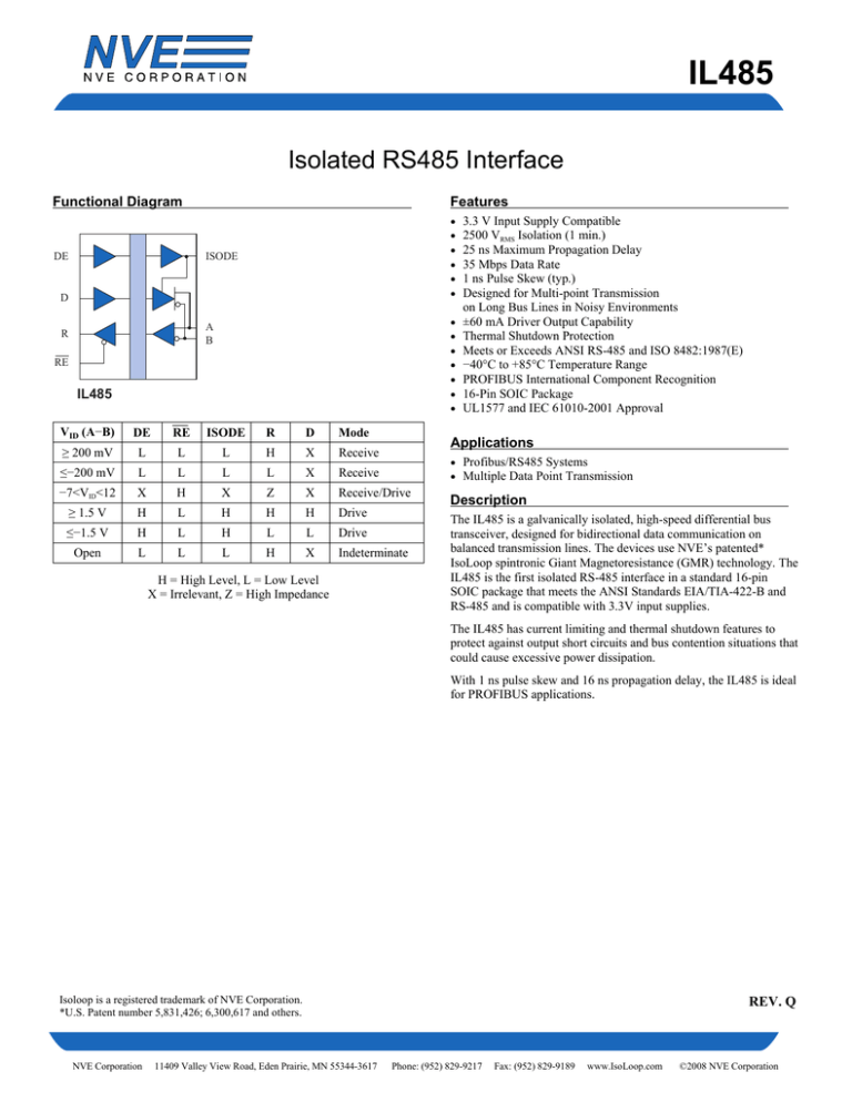
IL485 Isolated RS485 Interface Functional Diagram Features DE • • • • • • ISODE D • • • • • • • A B R RE IL485 VID (A−B) DE RE ISODE R D Mode ≥ 200 mV L L L H X Receive ≤−200 mV L L L L X Receive −7<VID<12 X H X Z X Receive/Drive ≥ 1.5 V H L H H H Drive ≤−1.5 V H L H L L Drive Open L L L H X Indeterminate H = High Level, L = Low Level X = Irrelevant, Z = High Impedance 3.3 V Input Supply Compatible 2500 VRMS Isolation (1 min.) 25 ns Maximum Propagation Delay 35 Mbps Data Rate 1 ns Pulse Skew (typ.) Designed for Multi-point Transmission on Long Bus Lines in Noisy Environments ±60 mA Driver Output Capability Thermal Shutdown Protection Meets or Exceeds ANSI RS-485 and ISO 8482:1987(E) −40°C to +85°C Temperature Range PROFIBUS International Component Recognition 16-Pin SOIC Package UL1577 and IEC 61010-2001 Approval Applications • Profibus/RS485 Systems • Multiple Data Point Transmission Description The IL485 is a galvanically isolated, high-speed differential bus transceiver, designed for bidirectional data communication on balanced transmission lines. The devices use NVE’s patented* IsoLoop spintronic Giant Magnetoresistance (GMR) technology. The IL485 is the first isolated RS-485 interface in a standard 16-pin SOIC package that meets the ANSI Standards EIA/TIA-422-B and RS-485 and is compatible with 3.3V input supplies. The IL485 has current limiting and thermal shutdown features to protect against output short circuits and bus contention situations that could cause excessive power dissipation. With 1 ns pulse skew and 16 ns propagation delay, the IL485 is ideal for PROFIBUS applications. Isoloop is a registered trademark of NVE Corporation. *U.S. Patent number 5,831,426; 6,300,617 and others. NVE Corporation 11409 Valley View Road, Eden Prairie, MN 55344-3617 REV. Q Phone: (952) 829-9217 Fax: (952) 829-9189 www.IsoLoop.com ©2008 NVE Corporation IL485 Absolute Maximum Ratings(11) Parameters Storage Temperature Ambient Operating Temperature Voltage Range at A or B Bus Pins Supply Voltage (1) Digital Input Voltage Digital Output Voltage Symbol TS TA VDD1, VDD2 Min. −65 −40 −7 −0.5 −0.5 −0.5 Typ. Continuous Total Power Dissipation Maximum Output Current Lead Solder Temperature ESD IO Max. 150 100 12 7 VDD + 0.5 VDD + 1 725 377 95 260 Units °C °C V V V V Max. 5.5 5.5 12 −7 Units VDD1 V 0.8 +12/−7 60 V V mA 8 mA 25°C 85°C mW mA °C kV 2 Test Conditions 10 sec. HBM Recommended Operating Conditions Parameters Input Voltage at any Bus Terminal (separately or common mode) Symbol VDD1 VDD2 VI VIC High-Level Digital Input Voltage VIH Low-Level Digital Input Voltage Differential Input Voltage (2) High-Level Output Current (Driver) High-Level Digital Output Current (Receiver) Low-Level Output Current (Driver) Low-Level Digital Output Current (Receiver) Ambient Operating Temperature Transient Immunity Digital Input Signal Rise and Fall Times VIL VID IOH Supply Voltage Min. 3.0 4.5 Typ. 2.4 3.0 0 IOH V V IOL −60 mA IOL −8 mA TA −40 20 85 tIR,tIF Test Conditions VDD1 = 3.3 V VDD1 = 5.0 V °C kV/μs DC Stable Insulation Specifications Parameters Creepage Distance Barrier Impedance Leakage Current Symbol Min. 8.08 Typ. Max. >1014||7 0.2 Units μA Test Conditions mm Ω || pF 240 VRMS, 60 Hz Safety and Approvals IEC61010-1 TUV Certificate Numbers: N1502812, N1502812-101 Classification: Reinforced Insulation Model IL485 Package 0.3" SOIC Pollution Degree II Material Group III Max. Working Voltage 300 VRMS UL 1577 Component Recognition Program File Number: E207481 Rated 2500VRMS for 1 minute Soldering Profile Per JEDEC J-STD-020C, MSL=2 2 NVE Corporation 11409 Valley View Road Eden Prairie, MN 55344-3617 USA Telephone: (952) 829-9217 Fax (952) 829-9189 Internet: www.isoloop.com IL485 IL485 Pin Connections 1 VDD1 Input Power Supply 2 GND1 Input Power Supply Ground Return 3 R 4 RE Read Data Enable (if RE is high, R = high impedance) VDD1 VDD2 5 DE Drive Enable GND1 GND2 6 D 7 NC 8 GND1 Input Power Supply Ground Return 9 GND2 Output Power Supply Ground Return 10 ISODE Isolated DE Output for use in Profibus applications where the state of the isolated drive enable node needs to be monitored 11 NC No Internal Connection 12 A Non-inverting Bus Line 13 B Inverting Bus Line 14 NC 15 GND2 Output Power Supply Ground Return. 16 VDD2 Output Power Supply Output Data from Bus Data Input to Bus R NC No Internal Connection RE B DE A NC D ISODE NC GND2 GND1 No Internal Connection 3 NVE Corporation 11409 Valley View Road Eden Prairie, MN 55344-3617 USA Telephone: (952) 829-9217 Fax (952) 829-9189 Internet: www.isoloop.com IL485 Driver Section Electrical Specifications are Tmin to Tmax and VDD = 4.5 V to 5.5 V, unless otherwise stated. Parameters Symbol Min. Typ.(5) Input Clamp Voltage VIK Output voltage VO 0 Differential Output Voltage(2) |VOD1| 1.5 Differential Output Voltage(2) |VOD2| 1.5 2.5 Differential Output Voltage(2)(6) VOD3 1.5 Change in Magnitude of Differential Δ|VOD| Output Voltage(7) Max. −1.5 6 6 5 5 Units V V V V V ±0.2 V RL = 54 Ω or 100 Ω VOC 3 −1 V RL = 54 Ω or 100 Ω Change in Magnitude of Common Mode Output Voltage(7) Δ|VOC| ±0.2 V RL = 54 Ω or 100 Ω Output Current(4) Output Disabled IO High Level Input Current Low Level Input Current IIH IIL Short-circuit Output Current IOS Common Mode Output Voltage Supply Current VDD1 = +5 V VDD1 = +3.3 V Parameters Maximum Data Rate Differential Output Prop Delay Pulse Skew(10) Differential Output Rise & Fall Time Output Enable Time To High Level Output Enable Time To Low Level Output Disable Time From High Level Output Disable Time From Low Level Skew Limit(3) IDD1 IDD1 Symbol tD(OD) tS(P) tT(OD) tPZH tPZL tPHZ tPLZ tSK(LIM) 4 3 Switching Specifications Min. Typ.(5) 35 16 1 8 31 22 28 16 2 1 −0.8 10 −10 250 −150 −250 6 4 Max. 25 6 10 65 35 50 32 12 Test Conditions IL = −18 mA IO = 0 IO = 0 RL = 54 Ω, VDD = 5 V RL = 54 Ω, VDD = 4.5 V VO = 12 V VO = −7 V VI = 3.5 V VI = 0.4 V VO = −6 V VO = 0 V VO = 8 V No Load (Outputs Enabled) mA μA μA mA mA Units Mbps ns ns ns ns ns ns ns ns Test Conditions RL = 54 Ω, CL = 50 pF RL = 54 Ω, CL = 50 pF RL = 54 Ω, CL = 50 pF RL = 54 Ω, CL = 50 pF RL = 54 Ω, CL = 50 pF RL = 54 Ω, CL = 50 pF RL = 54 Ω, CL = 50 pF RL = 54 Ω, CL = 50 pF RL = 54 Ω, CL = 50 pF Notes (apply to both driver and receiver sections): 1. All voltage values are with respect to network ground except differential I/O bus voltages. 2. Differential input/output voltage is measured at the noninverting terminal A with respect to the inverting terminal B. 3. Skew limit is the maximum propagation delay difference between any two devices at 25°C. 4. The power-off measurement in ANSI Standard EIA/TIA-422-B applies to disabled outputs only and is not applied to combined inputs and outputs. 5. All typical values are at VDD1,VDD2 = 5 V or VDD1= 3.3 V and TA = 25°C. 6. The minimum VOD2 with a 100 Ω load is either ½ VOD1 or 2 V, whichever is greater. 7. Δ|VOD| and Δ|VOC| are the changes in magnitude of VOD and VOC, respectively, that occur when the input is changed form one logic state to the other. 8. This applies for both power on and power off, refer to ANSI standard RS-485 for exact condition. The EIA/TIA-422-B limit does not apply for a combined driver and receiver terminal. 9. Includes 8 ns read enable time. Maximum propagation delay is 25 ns after read assertion. 10. Pulse skew is defined as |tPLH − tPHL| of each channel. 11. The relevant test and measurement methods are given in the Electromagnetic Compatibility section on p. 6. 12. External magnetic field immunity is improved by this factor if the field direction is “end-to-end” rather than to “pin-to-pin” (see diagram on p. 6). 4 NVE Corporation 11409 Valley View Road Eden Prairie, MN 55344-3617 USA Telephone: (952) 829-9217 Fax (952) 829-9189 Internet: www.isoloop.com IL485 Receiver Section Electrical Specifications are Tmin to Tmax and VDD = 4.5 V to 5.5 V, unless otherwise stated. Parameters Symbol Min. Typ.(5) Positive-going Input VIT+ Threshold Voltage Negative-going Input VIT−0.2 Threshold Voltage Hysteresis Voltage (VIT+ − VIT-) VHYS 60 Max. Units 0.2 V V mV VDD − 0.2 High Level Digital Output Voltage VOH Low Level Digital Output Voltage VOL 0.2 V High-impedance-state output current IOZ μA Line Input Current(8) II ±20 1 −0.8 Input Resistance rI Supply Current IDD2 12 V 20 27 Switching Characteristics at 5 V Min. Typ.(5) 35 mA 34 mA Max. Units Mbps Symbol Propagation Delay(2, 9) tPD 24 32 ns tSK(P) 1 6 ns 8 24 45 45 27 ns ns ns ns ns Max. Units Mbps (3) Skew Limit Output Enable Time To High Level Output Enable Time To Low Level Output Disable Time From High Level Output Disable Time From Low Level Parameters Maximum Data Rate Propagation Delay(2, 9) Pulse Skew(2, 10) (3) Skew Limit Output Enable Time to High Level Output Enable Time to Low Level Output Disable Time from High Level Output Disable Time from Low Level tSK(LIM) 2 tPZH 17 tPZL 30 tPHZ 30 tPLZ 18 Switching Characteristics at 3.3 V Symbol Min. Typ.(5) 35 VID = 200 mV IOH = −20 μA VID = −200 mV IOH = 20 μA VO = 0.4 to (VDD2−0.5) V VI = 12 V VI = −7 V Other Input(11) = 0 V kΩ Parameters Maximum Data Rate Pulse Skew(2, 10) Test Conditions VO = 2.7 V, IO = −0.4 mA VO = 0.5 V, IO = 8 mA tPD 27 32 ns tSK(P) 2 6 ns tSK(LIM) tPZH tPZL tPHZ tPLZ 4 20 33 33 20 8 24 45 45 27 ns ns ns ns ns No load Outputs Enabled Test Conditions RL = 54 Ω, CL = 50 pF VO = −1.5 V to 1.5 V, CL = 15 pF VO = −1.5 V to 1.5 V, CL = 15 pF RL = 54 Ω, CL = 50 pF CL = 15 pF CL = 15 pF CL = 15 pF CL = 15 pF Test Conditions RL = 54 Ω, CL = 50 pF VO = −1.5 V to 1.5 V, CL = 15 pF VO = −1.5 V to 1.5 V, CL = 15 pF RL = 54 Ω, CL = 50 pF CL = 15 pF CL = 15 pF CL = 15 pF CL = 15 pF Magnetic Field Immunity(11) Power Frequency Magnetic Immunity Pulse Magnetic Field Immunity Damped Oscillatory Magnetic Field Cross-axis Immunity Multiplier(12) HPF HPM HOSC KX Power Frequency Magnetic Immunity Pulse Magnetic Field Immunity Damped Oscillatory Magnetic Field Cross-axis Immunity Multiplier(12) HPF HPM HOSC KX Magnetic Field Immunity at 5 V 2800 3500 4000 4500 4000 4500 2.5 Magnetic Field Immunity at 3.3 V 1000 1500 1800 2000 1800 2000 2.5 A/m A/m A/m 50Hz/60Hz tp = 8µs 0.1Hz – 1MHz A/m A/m A/m 50Hz/60Hz tp = 8µs 0.1Hz – 1MHz 5 NVE Corporation 11409 Valley View Road Eden Prairie, MN 55344-3617 USA Telephone: (952) 829-9217 Fax (952) 829-9189 Internet: www.isoloop.com IL485 Application Information Electrostatic Discharge Sensitivity Dynamic Power Consumption This product has been tested for electrostatic sensitivity to the limits stated in the specifications. However, NVE recommends that all integrated circuits be handled with appropriate care to avoid damage. Damage caused by inappropriate handling or storage could range from performance degradation to complete failure. IsoLoop Isolators achieve their low power consumption from the way they transmit data across the isolation barrier. By detecting the edge transitions of the input logic signal and converting these to narrow current pulses, a magnetic field is created around the GMR Wheatstone bridge. Depending on the direction of the magnetic field, the bridge causes the output comparator to switch following the input logic signal. Since the current pulses are narrow, about 2.5 ns, the power consumption is independent of mark-to-space ratio and solely dependent on frequency. This has obvious advantages over optocouplers, which have power consumption heavily dependent on frequency and time. Electromagnetic Compatibility The IL485 is fully compliant with generic EMC standards EN50081, EN50082-1 and the umbrella line-voltage standard for Information Technology Equipment (ITE) EN61000. The IsoLoop Isolator’s Wheatstone bridge configuration and differential magnetic field signaling ensure excellent EMC performance against all relevant standards. NVE conducted compliance tests in the categories below: The approximate power supply current per channel is: IIN = 40 x EN50081-1 Residential, Commercial & Light Industrial Methods EN55022, EN55014 EN50082-2: Industrial Environment Methods EN61000-4-2 (ESD), EN61000-4-3 (Electromagnetic Field Immunity), EN61000-4-4 (Electrical Transient Immunity), EN61000-4-6 (RFI Immunity), EN61000-4-8 (Power Frequency Magnetic Field Immunity), EN61000-4-9 (Pulsed Magnetic Field), EN61000-4-10 (Damped Oscillatory Magnetic Field) ENV50204 Radiated Field from Digital Telephones (Immunity Test) f x 1 mA 4 fMAX Where f = operating frequency fMAX = 50 MHz Power Supply Decoupling Both VDD1 and VDD2 must be bypassed with 47 nF ceramic capacitors. These should be placed as close as possible to VDD pins for proper operation. Additionally, VDD2 should be bypassed with a 10 µF tantalum capacitor. Immunity to external magnetic fields is even higher if the field direction is “end-to-end” rather than to “pin-to-pin” as shown in the diagram below: Cross-axis Field Direction 6 NVE Corporation 11409 Valley View Road Eden Prairie, MN 55344-3617 USA Telephone: (952) 829-9217 Fax (952) 829-9189 Internet: www.isoloop.com IL485 0.3" 16-pin SOIC Package Dimensions in inches (mm) 0.287 (7.29) 0.300 (7.62) 0.013 (0.3) 0.020 (0.5) NOM 0.016 (0.4) 0.050 (1.3) 0.007 (0.2) 0.013 (0.3) 0.397 (10.1) 0.413 (10.5) 0.092 (2.34) 0.105 (2.67) Pin 1 identified by either an indent or a marked dot 0.394 (10.00) 0.419 (10.64) 0.08 (2.0) 0.10 (2.5) 0.040 (1.0) NOTE: Pin spacing is a BASIC 0.060 (1.5) dimension; tolerances do not accumulate 0.004 (0.1) 0.012 (0.3) Ordering Information and Valid Part Numbers IL 485 E TR13 Bulk Packaging Blank = Tube TR = 13'' Tape and Reel Valid Part Numbers IL485 IL485E Package Blank = 80/20 Tin/Lead Plating E = RoHS Compliant All IL485 part types are available on tape and reel. Base Part Number 485 = RS-485 Transceiver Product Family IL = Isolators RoHS COMPLIANT 7 NVE Corporation 11409 Valley View Road Eden Prairie, MN 55344-3617 USA Telephone: (952) 829-9217 Fax (952) 829-9189 Internet: www.isoloop.com IL485 ISB-DS-001-IL485-Q March 2008 Changes • Added magnetic field immunity and electromagnetic compatibility specifications. • Added note on package drawing that pin-spacing tolerances are non-accumulating. ISB-DS-001-IL485-P Changes • Changed ordering information to reflect that devices are now fully RoHS compliant with no exemptions. ISB-DS-001-IL485-O Changes • Reorganized supply current specifications; misc. minor changes ISB-DS-001-IL485-N Changes • ISB-DS-001-IL485-M Changes • ISB-DS-001-IL485-L Updated package drawing; misc. changes Changes • ISB-DS-001-IL485-J Updated open input state in truth table Changes • ISB-DS-001-IL485-K Eliminated soldering profile chart Update UL and IEC approvals Changes • Revision letter added. • Ordering Information Removed. • IEC 61010-1 “Reinforced Insulation” added. • Notes added. • PagIR Soldering Profile added • Ordering Information added. 8 NVE Corporation 11409 Valley View Road Eden Prairie, MN 55344-3617 USA Telephone: (952) 829-9217 Fax (952) 829-9189 Internet: www.isoloop.com IL485 About NVE An ISO 9001 Certified Company NVE Corporation manufactures innovative products based on unique spintronic Giant Magnetoresistive (GMR) technology. Products include Magnetic Field Sensors, Magnetic Field Gradient Sensors (Gradiometers), Digital Magnetic Field Sensors, Digital Signal Isolators, and Isolated Bus Transceivers. NVE pioneered spintronics and in 1994 introduced the world’s first products using GMR material, a line of ultra-precise magnetic sensors for position, magnetic media, gear speed and current sensing. NVE Corporation 11409 Valley View Road Eden Prairie, MN 55344-3617 USA Telephone: (952) 829-9217 Fax: (952) 829-9189 Internet: www.nve.com e-mail: isoinfo@nve.com The information provided by NVE Corporation is believed to be accurate. However, no responsibility is assumed by NVE Corporation for its use, nor for any infringement of patents, nor rights or licenses granted to third parties, which may result from its use. No license is granted by implication, or otherwise, under any patent or patent rights of NVE Corporation. NVE Corporation does not authorize, nor warrant, any NVE Corporation product for use in life support devices or systems or other critical applications, without the express written approval of the President of NVE Corporation. Specifications shown are subject to change without notice. ISB-DS-001-IL485-Q March 2008 9 NVE Corporation 11409 Valley View Road Eden Prairie, MN 55344-3617 USA Telephone: (952) 829-9217 Fax (952) 829-9189 Internet: www.isoloop.com
