A New Soft-Switched Resonant DC-DC Converter
advertisement

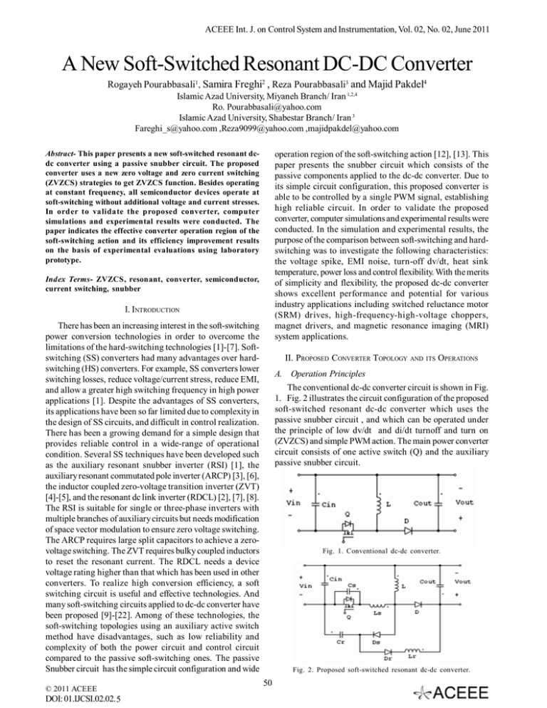
ACEEE Int. J. on Control System and Instrumentation, Vol. 02, No. 02, June 2011 A New Soft-Switched Resonant DC-DC Converter Rogayeh Pourabbasali1, Samira Freghi2 , Reza Pourabbasali3 and Majid Pakdel4 Islamic Azad University, Miyaneh Branch/ Iran 1,2,4 Ro. Pourabbasali@yahoo.com Islamic Azad University, Shabestar Branch/ Iran 3 Fareghi_s@yahoo.com ,Reza9099@yahoo.com ,majidpakdel@yahoo.com operation region of the soft-switching action [12], [13]. This paper presents the snubber circuit which consists of the passive components applied to the dc-dc converter. Due to its simple circuit configuration, this proposed converter is able to be controlled by a single PWM signal, establishing high reliable circuit. In order to validate the proposed converter, computer simulations and experimental results were conducted. In the simulation and experimental results, the purpose of the comparison between soft-switching and hardswitching was to investigate the following characteristics: the voltage spike, EMI noise, turn-off dv/dt, heat sink temperature, power loss and control flexibility. With the merits of simplicity and flexibility, the proposed dc-dc converter shows excellent performance and potential for various industry applications including switched reluctance motor (SRM) drives, high-frequency-high-voltage choppers, magnet drivers, and magnetic resonance imaging (MRI) system applications. Abstract- This paper presents a new soft-switched resonant dcdc converter using a passive snubber circuit. The proposed converter uses a new zero voltage and zero current switching (ZVZCS) strategies to get ZVZCS function. Besides operating at constant frequency, all semiconductor devices operate at soft-switching without additional voltage and current stresses. In order to validate the proposed converter, computer simulations and experimental results were conducted. The paper indicates the effective converter operation region of the soft-switching action and its efficiency improvement results on the basis of experimental evaluations using laboratory prototype. Index Terms- ZVZCS, resonant, converter, semiconductor, current switching, snubber I. INTRODUCTION There has been an increasing interest in the soft-switching power conversion technologies in order to overcome the limitations of the hard-switching technologies [1]-[7]. Softswitching (SS) converters had many advantages over hardswitching (HS) converters. For example, SS converters lower switching losses, reduce voltage/current stress, reduce EMI, and allow a greater high switching frequency in high power applications [1]. Despite the advantages of SS converters, its applications have been so far limited due to complexity in the design of SS circuits, and difficult in control realization. There has been a growing demand for a simple design that provides reliable control in a wide-range of operational condition. Several SS techniques have been developed such as the auxiliary resonant snubber inverter (RSI) [1], the auxiliary resonant commutated pole inverter (ARCP) [3], [6], the inductor coupled zero-voltage transition inverter (ZVT) [4]-[5], and the resonant dc link inverter (RDCL) [2], [7], [8]. The RSI is suitable for single or three-phase inverters with multiple branches of auxiliary circuits but needs modification of space vector modulation to ensure zero voltage switching. The ARCP requires large split capacitors to achieve a zerovoltage switching. The ZVT requires bulky coupled inductors to reset the resonant current. The RDCL needs a device voltage rating higher than that which has been used in other converters. To realize high conversion efficiency, a soft switching circuit is useful and effective technologies. And many soft-switching circuits applied to dc-dc converter have been proposed [9]-[22]. Among of these technologies, the soft-switching topologies using an auxiliary active switch method have disadvantages, such as low reliability and complexity of both the power circuit and control circuit compared to the passive soft-switching ones. The passive Snubber circuit has the simple circuit configuration and wide © 2011 ACEEE DOI: 01.IJCSI.02.02. 5 II. PROPOSED CONVERTER TOPOLOGY AND ITS OPERATIONS A. Operation Principles The conventional dc-dc converter circuit is shown in Fig. 1. Fig. 2 illustrates the circuit configuration of the proposed soft-switched resonant dc-dc converter which uses the passive snubber circuit , and which can be operated under the principle of low dv/dt and di/dt turnoff and turn on (ZVZCS) and simple PWM action. The main power converter circuit consists of one active switch (Q) and the auxiliary passive snubber circuit. Fig. 1. Conventional dc-dc converter. Fig. 2. Proposed soft-switched resonant dc-dc converter. 50 ACEEE Int. J. on Control System and Instrumentation, Vol. 02, No. 02, June 2011 of the proposed resonant dc-dc converter circuit is as follows: Mode 1 At mode 1, the active switch Q is turned on and a voltage nVin is reflected across the secondary winding of the main inductor. As a result, resonance based on Lr and Cr starts partially. The snubber capacitor voltage is discharged toward to low level. Mode 2 When the snubber capacitor voltage is fully discharged to zero, at this time, the additional operation mode of mode 2 is started, and the Cr current decreases linearly to release the resonant inductor energy. When the Cr current becomes zero, mode 3 starts. Mode 3 The main inductor energy is stored from the input side in this mode. When the active switch is turned off by the controller gate off signal of duty ratio (±), mode 4 starts Mode 4 At this mode, the turn-off voltage applied to the active switch is suppressed by the snubber capacitor, and then the turn-off loss of the active switch becomes small. When the capacitor voltage reaches to Vin +Vout , mode 5 starts. Mode 5 The energy stored in the main inductor is released to the output side in this mode. Since deep discharge of the snubber capacitor can be obtained at the condition of small value of Vout /Vin , the large reduction of the turn-off loss of the active switch can be achieved. This means that the higher input voltage at the output constant voltage control condition grants the larger effectiveness of the efficiency improvement. III. SIMULATION RESULTS The proposed two quadrant soft switched converter in the PSIM software environment is shown in Fig. 4. The following circuit parameters have been used in simulations: 1) A MOSFET module at 400V - 10A was used; 2) The resonant capacitor Cr used was 120 nF- 50V polypropylene capacitor; 3) The resonant inductor Lr used was 47 H ; 4) The snubber inductor Ls used was 10 H ; 5) The snubber capacitor Cs used was 1nF; 6) The input and output capacitors (Cin and Cout) used were 470 F ; 7) The diodes D and Dr used were 1N4500; 8) The resistance 1&! is used as a load. The waveforms of vds and ids of the switch Q is shown in Fig. 5. The output dc voltage (Vout) is shown in Fig. 6. The simulation results show that the proposed soft switched resonant dc-dc converter has the proper response. Fig. 3. Operation modes. A. Circuit Analysis Fig. 3 indicates operation mode transition diagram of the proposed soft-switched resonant dc-dc converter. Operation © 2011 ACEEE DOI: 01.IJCSI.02.02. 5 51 ACEEE Int. J. on Control System and Instrumentation, Vol. 02, No. 02, June 2011 Fig. 4. Proposed soft switched resonant dc-dc converter in PSIM software Fig. 7. Prototype of the proposed converter. Fig. 5. Vds and Ids waveforms of the switch. Fig. 8. Drain-source ( VDS ) signal: Volt/Div = 0.5 v, Time/Div= 10 s , Vin =3.66 v, I in=0.6A Fig. 6. Output dc voltage (Vout). simulation results show that the proposed soft switched resonant dc-dc converter has the proper response. IV. EXPERIMENTAL RESULTS A Prototype of the proposed converter, as shown in Fig. 7 has been built in the laboratory. The newly proposed converter operates with an input voltage Vs = 3.67V, output voltage Vo = 1V, load current of 0.6A and a switching frequency of 50 kHz. The VDS and VGS waveforms of MOSFET switch in a time period of one switching cycle are shown in Fig. 8 and Fig. 9 respectively. The voltage across resonant capacitor 120nF is shown in Fig. 10. The clock signal in a time period of one switching cycle is shown in Fig. 11. The output DC voltage is shown in Fig. 12. © 2011 ACEEE DOI: 01.IJCSI.02.02.5 Fig. 9. Gate signal: Volt/Div = 5v, Time/Div= 10 s , Vin =3.67 v, I in=0.6A 52 ACEEE Int. J. on Control System and Instrumentation, Vol. 02, No. 02, June 2011 simulations using PSIM software and experimental results were given. With the merits of simplicity and flexibility, the proposed soft switched dc-dc converter shows excellent performance and potential for various industry applications including switched reluctance motor (SRM) drives, high-frequency-high-voltage choppers, magnet drivers, and magnetic resonance imaging (MRI) system applications. The operation principle of the proposed circuit, its design consideration and efficiency characteristic are described on the basis of theoretical and experimental point of view. It is verified that the efficiency of the proposed new soft-switching converter increases when the passive snubber circuit is implemented compared to the hard-switching operation. REFERENCES Fig. 10. Voltage across resonant capacitor 120 nF: [1] J. S. Lai, R. W. Young, G. W. Ott, J. W. McKeever, and F. Z. Peng, “A Delta Configured Auxiliary Resonant Snubber Inverter,” IEEE Trans. on Ind. Appl., Vol. 32, No. 3, May/Jun. 1996, pp. 518–525. [2] D. M. Divan, “The Resonant DC Link Converter — A New Concept in Static Power Conversion,” in Conf. Rec. of IEEE-IAS, Oct. 1986, pp. 648-656. [3] W. McMurray, “Resonant Snubbers with Auxiliary Switches,” IEEE Trans. on Ind. Appl., Vol. 29, No. 2, Mar./Apr. 1993, pp. 355–362.2. [4] H. Mao and F. C. Lee, “Improvement on Zero-Voltage Transition Three-Phase Rectifier/Inverter,” in Proc. of VPEC’95 Seminar, Vol. 13, 1995, pp. 19-27. [5] J. P. Gegner and C. Q. Lee, “Zero-Voltage Transition Converters using Inductor Feedback Technique,” in Conf. Rec. of IEEE-APEC, Orlando, FL, Mar. 1994, pp. 862-868. [6] R. W. De Doncker and J. P. Lyons, “The Auxiliary Resonant Commutated Pole Converters,” in Conf. Rec. of IEEE-IAS, 1990, pp. 1228-1235. [7] J. He and N. Mohan, “ Parallel Resonant DC Link Circuit – A Novel Zero Switching Losses Topology with Minimum Voltage Stresses,” in Conf. Rec. of IEEE-PESC, 1989, pp. 1006- 1012. [8] R. Redl, N. O. Sokal, and L. Balogh, “A novel soft-switching full-bridge dc/dc converter: Analysis, design considerations, and experimental results at 1.5 kW, 100 kHz,” IEEE Trans. Power Electron., vol. 6, no. 3, pp. 408– 418, Jul. 1991. [9] A. Elasser and D.A. Torrey, “Soft switching active snubbers for DC/DC converters”, IEEE Trans. Power Electron., vol. 11, No. 5, pp. 710-722, Sep. 1996. [10] G. Ioannidis, E. Xanthoulis and S.N. Manias, “Analysis and design of a novel fixed-frequency buck-boost zero-current zerovoltage switched converter”, Proc. IEE—Elect. Power Appl., Vol. 145, No. 1, pp. 33-38, Jan. 1998. [11] K.M. Smith Jr and K.M. Smedley, “Engineering design of lossless passive soft switching methods for PWM converters – part II. With non-minimum voltage stress circuit cells”, IEEE Trans. Power Electron., Vol. 17, No. 6, pp. 864-873, Nov. 2002. [12] Z. Lin, “A passive regenerative soft-switching converter with the simplest topology”, in Proc. IEEE Power Electronics Specialists Conf., 2002, pp.949-954. [13] C.Y. Inaba, Y. Konishi and M. Nakaoka, “High-frequency flybacktype soft-switching PWM DC-DC power converter with energy recovery transformer and auxiliary passive lossless snubbers”, Proc. IEE—Elect. Power Appl., Vol. 151, N0. 1, pp. 3237, Jan. 2004. Volt/Div = 50 mv, Time/Div= 10 s , Vin =3.62 v, I in=0.6A Fig. 11. The clock signal: Volt/Div = 1 v, Time/Div= 10 s , Vin =3.67 v, I in=0.6A Fig. 12. The output DC voltage: Volt/Div = 1 v, Time/Div= 0.5 ms, Vin =3.67 v, I in=0.6A V. CONCLUSION In this section, a new soft-switching converter topology with a simple resonant snubber circuit was proposed and was verified fully for working conditions with a load. In order to verify performance of the proposed converter, circuit © 2011 ACEEE DOI: 01.IJCSI.02.02.5 53 ACEEE Int. J. on Control System and Instrumentation, Vol. 02, No. 02, June 2011 [14] B. Choi,W. Lim, S. Bang, and S. Choi, “Small-signal analysis and control design of asymmetrical half-bridge DC-DC converters,” IEEE Trans. Ind. Electron., vol. 53, no. 2, pp. 511–520, Apr. 2006. [15] J.-J. Lee and B.-H. Kwon, “DC-DC converter using a multiplecoupled inductor for low output voltages,” IEEE Trans. Ind. Electron., vol. 54, no. 1, pp. 467–478, Feb. 2007. [16] S.-S. Lee, S.-K. Han, and G.-W. Moon, “Analysis and design of asymmetrical ZVS PWM half bridge forward converter with flyback type transformer,” in Proc. IEEE Power Electron. Spec. Conf., 2004, vol. 2, pp. 1525–1530. [17] L. H. Dixon, “Magnetics design for switching power supplies,” Unitrode Seminar, 2001. © 2011 ACEEE DOI: 01.IJCSI.02.02. 5 [18] Kh. Rahimi kh., M. Pakdel, “A New ZVZCS Isolated DC-DC Converter,” in Proc. IEEE ICIT2009. Conf., Australia, Feb. 2009. [19] Y.Chul Ryu; Y.Woong Hwang, “A new soft-start method with abnormal over current protection function for switching power supplies ,” IEMDC.2005.195757, 2005, pp. 421-425. [20] Konishi, Y., Huang, Y.F., “Soft-switching buck boost converter using pulse current regenerative resonant snubber,” IET, 2007, pp. 127-128. [21] Barreto, L.H.S.C., Sebastiao, M.G., de Freitas, L.C., Coelho, E.A.A., Farias, V.J., Vieira, J.B., Jr., “Analysis of a soft-switched PFC boost converter using analog and digital control circuits,” IEEE Trans. Ind. Elect., 2005, pp. 221-227. [22] Dong Cao; Fang Zheng Peng, “A family of zero current switching switched-capacitor dc-dc converters,” APEC.2010.5433407, 2010, pp. 1365-1372. 54


