IS31AP4066D
DUAL 1.3W STEREO AUDIO AMPLIFIER
January 2014
GENERAL DESCRIPTION
KEY SPECIFICATIONS
The IS31AP4066D is a dual bridge-connected audio
power amplifier which, when connected to a 5V supply,
will deliver 1.3W to an 8Ω load.
The IS31AP4066D features a low-power consumption
shutdown mode and thermal shutdown protection. It
also utilizes circuitry to reduce “click-and-pop” during
device turn-on.
PO at RL = 8Ω, VCC = 5V
THD+N = 1% ---------------------- 1.3W (Typ.)
THD+N = 10% --------------------- 1.6W (Typ.)
PO at RL = 8Ω, VCC = 4V
THD+N = 1% ----------------------- 0.81W (Typ.)
Shutdown current ------------------- 0.3μA (Typ.)
Supply voltage range --------------- 2.7V ~ 5.5V
QFN-16 (3mm × 3mm) package
APPLICATIONS
FEATURES
Cell phones, PDA, MP4,PMP
Portable and desktop computers
Desktops audio system
Multimedia monitors
Suppress “click-and-pop”
Thermal shutdown protection circuitry
Micro power shutdown mode
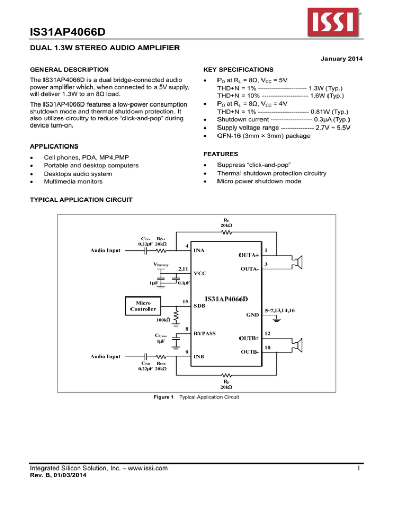
TYPICAL APPLICATION CIRCUIT
Figure 1
Integrated Silicon Solution, Inc. – www.issi.com
Rev. B, 01/03/2014
Typical Application Circuit
1
IS31AP4066D
PIN CONFIGURATION
16 GND
15 SDB
14 GND
13 GND
GND 6
GND 7
BYPASS 8
Pin Configuration (Top View)
5
Package
GND
QFN-16
PIN DESCRIPTION
No.
Pin
Description
1
OUTA+
Left channel positive output.
2,11
VCC
Supply voltage.
3
OUTA-
Left channel negative output.
4
INA
Left channel input.
5~7,13,14,16
GND
Ground.
8
BYPASS
Bypass capacitor which provides the
common mode voltage.
9
INB
Right channel input.
10
OUTB-
Right channel negative output.
12
OUTB+
Right channel positive output.
15
SDB
Shutdown control, hold low for shutdown
mode.
Thermal Pad
Connect to GND.
Integrated Silicon Solution, Inc. – www.issi.com
Rev. B, 01/03/2014
2
IS31AP4066D
ORDERING INFORMATION
Industrial Range: -40°C to +85°C
Order Part No.
Package
QTY/Reel
IS31AP4066D-QFLS2-TR
QFN-16, Lead-free
2500
Copyright © 2014 Integrated Silicon Solution, Inc. All rights reserved. ISSI reserves the right to make changes to this specification and its products at any time without notice. ISSI assumes no liability arising out of the application or use of any information, products or services described herein. Customers are advised to obtain the latest version of this device specification before relying on any published information and before placing orders for products. Integrated Silicon Solution, Inc. does not recommend the use of any of its products in life support applications where the failure or malfunction of the product can reasonably be expected to cause failure of the life support system or to significantly affect its safety or effectiveness. Products are not authorized for use in such applications unless Integrated Silicon Solution, Inc. receives written assurance to its satisfaction, that: a.) the risk of injury or damage has been minimized; b.) the user assume all such risks; and c.) potential liability of Integrated Silicon Solution, Inc is adequately protected under the circumstances
Integrated Silicon Solution, Inc. – www.issi.com
Rev. B, 01/03/2014
3
IS31AP4066D
ABSOLUTE MAXIMUM RATINGS
Supply voltage, VCC
Voltage at any input pin
Maximum junction temperature, TJMAX
Storage temperature range, TSTG
Operating temperature range, TA
ESD (HBM)
ESD (CDM)
-0.3V ~ +6.0V
-0.3V ~ VCC+0.3V
150°C
-65°C ~ +150°C
−40°C ~ +85°C
1kV
1kV
Note:
Stresses beyond those listed under “Absolute Maximum Ratings” may cause permanent damage to the device. These are stress ratings only and
functional operation of the device at these or any other condition beyond those indicated in the operational sections of the specifications is not
implied. Exposure to absolute maximum rating conditions for extended periods may affect device reliability.
ELECTRICAL CHARACTERISTICS
The following specifications apply for VCC= 5V, unless otherwise noted.
Limits apply for TA = 25°C. (Note 1 or specified)
Symbol
Parameter
Condition
Min.
Typ.
2.7
Max.
Unit
5.5
V
VCC
Supply voltage
ICC
Quiescent power supply current
VIN = 0V, IO = 0A
3.9
10.0
mA
ISD
Shutdown current
GND applied to the shutdown pin
0.3
2.5
μA
VIH
Shutdown input voltage high
VIL
Shutdown input voltage low
tWU
Turn on time
1.4
V
0.4
CBypass = 1μF (Note 2)
120
V
ms
ELECTRICAL CHARACTERISTICS OPERATION
The following specifications apply for VCC= 5V, unless otherwise noted.
Limits apply for TA = 25°C. (Note 2 or specified)
Symbol
Parameter
VOS
Output offset voltage
Po
Output power
THD+N
PSRR
Total harmonic
distortion +noise
Power supply rejection
ratio
Condition
Min.
Typ.
Max.
Unit
VIN = 0V
5.0
25.0
mV
THD+N = 1%, f = 1kHz, RL= 8Ω
1.3
W
THD+N = 10%, f = 1kHz, RL = 8Ω
1.6
W
f = 1kHz, AV = 2, RL = 8Ω, PO = 1W
0.1
%
Input floating, 217Hz, VRipple = 200mVp-p
CBypass = 1μF, RL = 8Ω
80.0
dB
Input floating 1kHz, VRipple = 200mVp-p
CBypass = 1μF, RL = 8Ω
70.0
dB
Input GND 217Hz, VRipple = 200mVp-p
CBypass = 1μF, RL =8Ω
60.0
dB
Input GND 1kHz VRipple = 200mVp-p
CBypass = 1μF, RL = 8Ω
60.0
dB
XTalk
Channel separation
f = 1kHz, CBypass = 1μF
-100
dB
VNO
Output noise voltage
1kHz, A-weighted
7.0
μV
Integrated Silicon Solution, Inc. – www.issi.com
Rev. B, 01/03/2014
4
IS31AP4066D
ELECTRICAL CHARACTERISTICS
The following specifications apply for VCC= 3V, unless otherwise noted.
Limits apply for TA = 25°C. (Note 1 or specified)
Symbol
Parameter
Condition
ICC
Quiescent power supply current
ISD
Shutdown current
VIH
Shutdown input voltage high
VIL
Shutdown input voltage low
tWU
Turn on time
Min.
Typ.
Max.
Unit
VIN = 0V, IO = 0A
2.6
6.5
mA
GND applied to the shutdown pin
0.1
2.2
μA
1.1
V
0.4
CBypass = 1μF (Note 2)
110
V
ms
ELECTRICAL CHARACTERISTICS OPERATION
The following specifications apply for VCC= 3V, unless otherwise noted.
Limits apply for TA = 25°C. (Note 2 or specified)
Symbol
Parameter
VOS
Output offset voltage
Po
Output power
THD+N
PSRR
Total harmonic
distortion+noise
Power supply
rejection ratio
Condition
Min.
Typ.
Max.
Unit
VIN = 0V
2.5
25.0
mV
THD+N = 1%, f = 1kHz, RL= 8Ω
0.5
W
THD+N = 10%, f = 1kHz, RL = 8Ω
0.6
W
f = 1kHz, AV = 2, RL = 8Ω, PO = 0.3W
0.1
%
Input floating, 217Hz, VRipple = 200mVp-p
CBypass = 1μF, RL = 8Ω
75.0
dB
Input floating 1kHz, VRipple = 200mVp-p
CBypass = 1μF, RL = 8Ω
70.0
dB
Input GND 217Hz, VRipple = 200mVp-p
CBypass = 1μF, RL =8Ω
62.0
dB
Input GND 1kHz VRipple = 200mVp-p
CBypass = 1μF, RL = 8Ω
62.0
dB
XTalk
Channel separation
f = 1kHz, CBypass = 1μF
-100
dB
VNO
Output noise voltage
1kHz, A-weighted
7.0
uV
Note1: All parameters are production tested at 25°C, functional operation of the device and parameters specified over other temperature range,
are guaranteed by design, characterization and process control.
Note 2: Guaranteed by design.
Integrated Silicon Solution, Inc. – www.issi.com
Rev. B, 01/03/2014
5
IS31AP4066D
TYPICAL PERFORMANCE CHARACTERISTICS
Vcc = 3V
RL
f = 1kHz
Vcc = 5V
RL
f = 1kHz
Figure 2
THD+N vs. Output Power
Vcc = 5V
RL
Po = 1W
Figure 4
THD+N vs. Output Power
Vcc = 3V
RL
Po=300mW
THD+N vs. Frequency
Figure 5
THD+N vs. Frequency
Vcc = 3V
RL
Input GND
Vcc = 5V
RL
Input GND
Figure 6
Figure 3
PSRR vs. Frequency
Integrated Silicon Solution, Inc. – www.issi.com
Rev. B, 01/03/2014
Figure 7
PSRR vs. Frequency
6
IS31AP4066D
Vcc = 5V
RL
Vcc = 5V
RL
Input Floating
Figure 8
PSRR vs. Frequency
Vcc = 3V
RL
Input Floating
Figure 10
Crosstalk vs. Frequency
Vcc = 5V
RL
A-Weighting
Figure 11
PSRR vs. Frequency
Noise Floor
Vcc = 3V
RL
Vcc = 5V
RL
Figure 12
Figure 9
Frequency Response
Integrated Silicon Solution, Inc. – www.issi.com
Rev. B, 01/03/2014
Figure 13
Frequency Response
7
IS31AP4066D
Vcc = 3V
RL
Vcc = 3V
RL
A-Weighting
Figure 14
Crosstalk vs. Frequency
Figure 15
Noise Floor
RL
Top Side
Bottom Side
Vcc = 5V
RL
f = 1kHz
Output Power (W)
Figure 16
Dropout Voltage vs. Supply Voltage
Figure 17
Power Dissipation vs. Output Power
RL
f = 1kHz
THD+N = 10%
THD+N = 1%
Figure18
Output Power vs. Supply Voltage
Integrated Silicon Solution, Inc. – www.issi.com
Rev. B, 01/03/2014
8
IS31AP4066D
FUNCTIONAL BLOCK DIAGRAM
VCC
INA
OUTA-
OUTA+
BYPASS
SDB
OUTB+
OUTB-
INB
GND
Integrated Silicon Solution, Inc. – www.issi.com
Rev. B, 01/03/2014
9
IS31AP4066D
APPLICATION INFORMATION
EXPOSED-DAP PACKAGE PCB MOUNTING
CONSIDERATIONS
The IS31AP4066D’s QFN (die attach paddle) package
provides a low thermal resistance between the die and
the PCB to which the part is mounted and soldered.
This allows rapid heat transfer from the die to the
surrounding PCB copper traces, ground plane and,
finally, surrounding air.
The QFN package must have it’s DAP soldered to a
copper pad on the PCB. The DAP’s PCB copper pad is
connected to a large plane of continuous unbroken
copper. This plane forms a thermal mass and heat sink
and radiation area. Place the heat sink area on either
outside plane in the case of a two-sided PCB, or on an
inner layer of a board with more than two layers.
BRIDGE CONFIGURATION EXPLANATION
As shown in Figure 1, the IS31AP4066D consists of
two pairs of operational amplifiers, forming a
two-channel (Channel A and Channel B) stereo
amplifier. External feedback resistors RF and input
resistors RIN set the closed-loop gain of Amp A (OUT-)
and Amp B OUT-) whereas two internal 20kΩ resistors
set Amp A’s (OUT+) and Amp B’s (OUT+) gain at 1.
The IS31AP4066D drives a load, such speaker,
connected between the two amplifier outputs, OUTA−
and OUTA+.
Figure 1 shows that Amp A’s (OUT-) output serves as
Amp A’s (OUT+) input. This results in both amplifiers
producing signals identical in magnitude, but 180° out
of phase. Taking advantage of this phase difference, a
load is placed between OUTA− and OUTA+ and driven
differentially (commonly referred to as “bridge mode”).
This results in a differential gain of
AV = 2×(RF/RIN)
(1)
Bridge mode amplifiers are different from single-ended
amplifiers that drive loads connected between a single
amplifier’s output and ground. For a given supply
voltage, bridge mode has a distinct advantage over the
single-ended configuration: its differential output
doubles the voltage swing across the load. This
produces four times the output power when compared
to a single-ended amplifier under the same conditions.
This increase in attainable output power assumes that
the amplifier is not current limited
Another advantage of the differential bridge output is
no net DC voltage across the load. This is
accomplished by biasing Channel A’s and Channel B’s
outputs at half-supply. This eliminates the coupling
capacitor that single supply, single ended amplifiers
require. Eliminating an output coupling capacitor in a
single-ended configuration forces a single-supply
amplifier’s half-supply bias voltage across the load.
This increases internal IC power dissipation and may
permanently damage loads such as speakers.
Integrated Silicon Solution, Inc. – www.issi.com
Rev. B, 01/03/2014
POWER SUPPLY BYPASSING
As with any power amplifier, proper supply bypassing
is critical for low noise performance and high power
supply rejection. Applications that employ a 5V
regulator typically use a 10μF in parallel with a 0.1μF
filter capacitor to stabilize the regulator’s output,
reduce noise on the supply line, and improve the
supply’s transient response. However, their presence
does not eliminate the need for a local 1.0μF tantalum
bypass capacitance connected between the
IS31AP4066D’s supply pins and ground. Keep the
length of leads and traces that connect capacitors
between the IS31AP4066D’s power supply pin and
ground as short as possible.
MICRO-POWER SHUTDOWN
The voltage applied to the SDB pin controls the
IS31AP4066D’s shutdown function. Activate
micro-power shutdown by applying GND to the SDB
pin. When active, the IS31AP4066D’s micro-power
shutdown feature turns off the amplifier’s bias circuitry,
reducing the supply current. The low 0.3μA typical
shutdown current is achieved by applying a voltage
that is as near as GND as possible to the SDB pin.
There are a few ways to control the micro-power
shutdown. These include using a single-pole,
single-throw switch, a microprocessor, or a
microcontroller. When use a switch, connect an
external 100kΩ resistor between the SDB pin and
GND. Select normal amplifier operation by closing the
switch. Opening the switch sets the SDB pin to ground
through the 100kΩ resistor, which activates the
micropower shutdown. The switch and resistor
guarantee that the SDB pin will not float. This prevents
unwanted state changes. In a system with a
microprocessor or a microcontroller, use a digital
output to apply the control voltage to the SDB pin.
Driving the SDB pin with active circuitry eliminates the
pull up resistor.
SELECTING PROPER EXTERNAL COMPONENTS
Optimizing the IS31AP4066D’s performance requires
properly selecting external components. Though the
IS31AP4066D operates well when using external
components with wide tolerances, best performance is
achieved by optimizing component values.
The IS31AP4066D is unity-gain stable, giving a
designer maximum design flexibility. The gain should
be set to no more than a given application requires.
This allows the amplifier to achieve minimum THD+N
and maximum signal-to-noise ratio. These parameters
are compromised as the closed-loop gain increases.
However, low gain demands input signals with greater
voltage swings to achieve maximum output power.
Fortunately, many signal sources such as audio
CODECs have outputs of 1VRMS (2.83VP-P). Please
10
IS31AP4066D
refer to the Audio Power Amplifier Design section for
more information on selecting the proper gain.
INPUT CAPACITOR VALUE SELECTION
Amplifying the lowest audio frequencies requires high
value input coupling capacitors CIN in Figure 1. A high
value capacitor can be expensive and may
compromise space efficiency in portable designs. In
many cases, however, the speakers used in portable
systems, whether internal or external, have little ability
to reproduce signals below 150Hz. Applications using
speakers with this limited frequency response reap
little improvement by using large input capacitor.
Besides effecting system cost and size, CIN have an
effect on the IS31AP4066D’s click and pop
performance. When the supply voltage is first applied,
a transient (pop) is created as the charge on the input
capacitor changes from zero to a quiescent state. The
magnitude of the pop is directly proportional to the
input capacitor’s size. Higher value capacitors need
more time to reach a quiescent DC voltage (usually
VCC/2) when charged with a fixed current. The
amplifier’s output charges the input capacitor through
the feedback resistors, RF. Thus, pops can be
minimized by selecting an input capacitor value that is
no higher than necessary to meet the desired −3dB
frequency.
A shown in Figure 1, the input resistors RIN and the
input capacitors CIN produce a −3dB high pass filter
cutoff frequency that is found using Equation (2).
f-3dB = 1/2πRINCIN
(2)
As an example when using a speaker with a low
frequency limit of 150Hz, CINA, using Equation (2) is
0.053μF. The 0.33μF CINA allows the IS31AP4066D to
drive high efficiency, full range speaker whose
response extends below 30Hz.
Choosing CBYPASS equal to 1.0μF along with a small
value of CIN (in the range of 0.1μF to 0.39μF),
produces a click-less and pop-less shutdown function.
As discussed above, choosing CIN no larger than
necessary for the desired band with helps minimize
click-and-pop. Connecting a 1μF capacitor, CBYPASS,
between the BYPASS pin and ground improves the
internal bias voltage’s stability and improves the
amplifier’s PSRR.
OPTIMIZING CLICK-AND-POP REDUCTION
PERFORMANCE
The IS31AP4066D contains circuitry that minimizes
turn-on and shutdown transients or “click-and-pop”.
For this discussion, turn-on refers to either applying
the power supply voltage or when the shutdown mode
is deactivated. When the part is turned on, an internal
current source changes the voltage of the BYPASS pin
in a controlled, linear manner. Ideally, the input and
outputs track the voltage applied to the BYPASS pin.
The gain of the internal amplifiers remains unity until
the voltage on the bypass pin reaches 1/2VCC. As soon
as the voltage on the bypass pin is stable, the device
becomes fully operational. Although the BYPASS pin
current cannot be modified, changing the size of
CBYPASS alters the device’s turn-on time and the
magnitude of “click-and-pop”. Increasing the value of
CBYPASS reduces the magnitude of turn-on pops.
However, this presents a tradeoff: as the size of
CBYPASS increases, the turn-on time increases. There is
a linear relationship between the size of CBYPASS and
the turn-on time. Here are some typical turn-on times
for various values of CBYPASS (all tested at VCC = 5V):
CBYPASS
tON
0.01μF
13ms
0.1μF
26ms
BYPASS CAPACITOR VALUE SELECTION
0.22μF
44ms
Besides minimizing the input capacitor size, careful
consideration should be paid to value of CBYPASS, the
capacitor connected to the BYPASS pin. Since CBYPASS
determines how fast the IS31AP4066D settles to
quiescent operation, its value is critical when
minimizing turn-on pops. The slower the
IS31AP4066D’s outputs ramp to their quiescent DC
voltage (nominally 1/2VCC), the smaller the turn-on pop.
0.47μF
68ms
1.0μF
120 ms
Integrated Silicon Solution, Inc. – www.issi.com
Rev. B, 01/03/2014
In order eliminate “click-and-pop”; all capacitors must
be discharged before turn-on. Rapidly switching VCC
on and off may not allow the capacitors to fully
discharge, which may cause “click-and-pop”.
11
IS31AP4066D
CLASSIFICATION REFLOW PROFILES
Profile Feature
Pb-Free Assembly
Preheat & Soak
Temperature min (Tsmin)
Temperature max (Tsmax)
Time (Tsmin to Tsmax) (ts)
150°C
200°C
60-120 seconds
Average ramp-up rate (Tsmax to Tp)
3°C/second max.
Liquidous temperature (TL)
Time at liquidous (tL)
217°C
60-150 seconds
Peak package body temperature (Tp)*
Max 260°C
Time (tp)** within 5°C of the specified
classification temperature (Tc)
Max 30 seconds
Average ramp-down rate (Tp to Tsmax)
6°C/second max.
Time 25°C to peak temperature
8 minutes max.
Figure 19
Classification Profile
Integrated Silicon Solution, Inc. – www.issi.com
Rev. B, 01/03/2014
12
IS31AP4066D
PACKAGE INFORMATION
QFN-16
Note: All dimensions in millimeters unless otherwise stated.
Integrated Silicon Solution, Inc. – www.issi.com
Rev. B, 01/03/2014
13
