DATASHEET
ICS514
LOCO™ PLL CLOCK GENERATOR
Description
Features
The ICS514 LOCOTM is the most cost effective way to
generate a high-quality, high-frequency clock output
from a 14.31818 MHz crystal or clock input. The name
LOCO stands for Low Cost Oscillator, as it is designed
to replace crystal oscillators in most electronic
systems. Using Phase-Locked Loop (PLL) techniques,
the device uses a standard, inexpensive crystal to
produce output clocks up to 66.66 MHz.
•
•
•
•
•
•
•
•
•
•
•
•
•
•
Stored in the chip’s ROM is the ability to generate five
different output frequencies, allowing one chip to work
in different speed processor systems.
The device also has a power-down mode that turns off
the clock outputs when both select pins are low. In this
mode, the internal PLL is not running.
Packaged as 8-pin SOIC or die
Pb (lead) free package
IDT’s lowest cost PLL clock plus reference
Produces common computer frequencies
Input crystal frequency typically 14.3182 MHz
Output clock frequencies up to 66.66 MHz from a
14.3182 MHz crystal or input clock
Low jitter of 50 ps (one sigma)
Compatible with all popular CPUs
Duty cycle of 45/55
Custom frequencies available
Operating voltage of 3.3 V to 5.5 V
Power-down mode turns off chip
25 mA drive capability at TTL levels
Advanced, low-power CMOS process
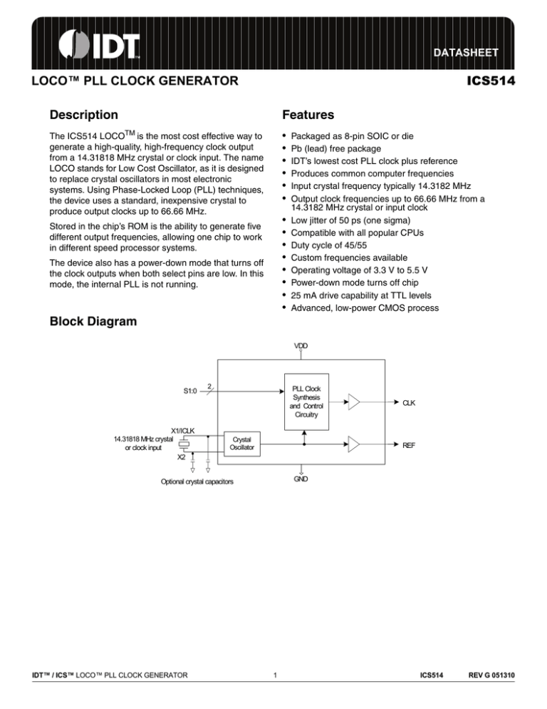
Block Diagram
VDD
S1:0
X1/ICLK
14.31818 MHz crystal
or clock input
X2
2
PLL Clock
Synthesis
and Control
Circuitry
Crystal
Oscillator
REF
GND
Optional crystal capacitors
IDT™ / ICS™ LOCO™ PLL CLOCK GENERATOR
CLK
1
ICS514
REV G 051310
ICS514
LOCO™ PLL CLOCK GENERATOR
CLOCK MULTIPLIER
Pin Assignment
Clock Decoding Table (MHz) with 14.31818
MHz Crystal or Clock Input
X1/ I CLK
1
8
X2
S1
S0
CLK
Multiplier
Accuracy
VDD
2
7
S1
0
0
Power-down CLK
—
—
GND
3
6
S0
REF
5
4
CLK
8 - p i n ( 1 5 0 mi l ) S OI C
0
1
25
1.746
1 ppm
M
0
33.33
2.328
0.008%
M
1
40
2.794
1 ppm
1
0
50
3.492
1 ppm
1
1
66.66
4.656
0.008%
0 = connect directly to ground
1 = connect directly to VDD
M = leave unconnected (floating)
CLK and REF stop low in power-down state
Pin Descriptions
Pin
Number
Pin
Name
Pin
Type
Pin Description
1
XI/ICLK
Input
Crystal connection to a 14.31818 MHz crystal or clock input.
2
VDD
Power
Connect to +3.3 V or +5 V.
3
GND
Power
Connect to ground.
4
REF
Output
Reference 14.31818 MHz crystal oscillator buffered clock output.
5
CLK
Output
Clock output per table above.
6
S0
Tri-level Input
Select 0 for output clock. Connect to GND or VDD or float. See
table above.
7
S1
Tri-level Input
Select 1 for output clock. Connect to GND or VDD or float. See
table above.
8
X2
Output
Crystal connection to a 14.31818 MHz crystal. Leave unconnected
for clock input.
Notes:
1. With S1 = S0 = 0, the internal PLL is turned off and the CLK outputs stops low. The crystal oscillator and
REF output are still active.
2. With a clock input, the phase relationship between the input and the output clocks can change each time
the device is powered on. If a fixed phase relationship is required, use the ICS571 or other zero delay
multipliers.
IDT™ / ICS™ LOCO™ PLL CLOCK GENERATOR
2
ICS514
REV G 051310
ICS514
LOCO™ PLL CLOCK GENERATOR
CLOCK MULTIPLIER
External Components
X2 to ground. These capacitors are used to adjust the
stray capacitance of the board to match the nominally
required crystal load capacitance. Because load
capacitance can only be increased in this trimming
process, it is important to keep stray capacitance to a
minimum by using very short PCB traces (and no vias)
between the crystal and device. Crystal capacitors, if
needed, must be connected from each of the pins X1
and X2 to ground.
Decoupling Capacitor
As with any high-performance mixed-signal IC, the
ICS514 must be isolated from system power supply
noise to perform optimally.
A decoupling capacitor of 0.01µF must be connected
between VDD and the GND. It must be connected close
to the ICS514 to minimize lead inductance. No external
power supply filtering is required for the ICS514.
The value (in pF) of these crystal caps should equal (CL
-12 pF)*2. In this equation, CL= crystal load capacitance
in pF. Example: For a crystal with a 16 pF load
capacitance, each crystal capacitor would be 8 pF
[(16-12) x 2 = 8].
Series Termination Resistor
A 33Ω terminating resistor can be used next to the CLK
and REF pins for trace lengths over one inch.
Crystal Load Capacitors
The total on-chip capacitance is approximately 12 pF. A
parallel resonant, fundamental mode crystal should be
used. The device crystal connections should include
pads for small capacitors from X1 to ground and from
Absolute Maximum Ratings
Stresses above the ratings listed below can cause permanent damage to the ICS514. These ratings, which
are standard values for IDT commercially rated parts, are stress ratings only. Functional operation of the
device at these or any other conditions above those indicated in the operational sections of the
specifications is not implied. Exposure to absolute maximum rating conditions for extended periods can
affect product reliability. Electrical parameters are guaranteed only over the recommended operating
temperature range.
Item
Rating
Supply Voltage, VDD
7V
All Inputs and Outputs (referenced to GND)
-0.5 V to VDD+0.5 V
Ambient Operating Temperature
0 to +70° C
Storage Temperature
-65 to +150° C
Soldering Temperature
260° C
IDT™ / ICS™ LOCO™ PLL CLOCK GENERATOR
3
ICS514
REV G 051310
ICS514
LOCO™ PLL CLOCK GENERATOR
CLOCK MULTIPLIER
Recommended Operation Conditions
Parameter
Min.
Max.
Units
0
+70
°C
+3.0
+5.5
V
Ambient Operating Temperature
Power Supply Voltage (measured in respect to GND)
Typ.
DC Electrical Characteristics
VDD=5.0 V ±5% , Ambient temperature 0 to +70° C, unless stated otherwise
Parameter
Symbol
Operating Voltage
Conditions
Min.
VDD
Max.
Units
5.5
V
3.0
Input High Voltage, ICLK only
VIH
ICLK (pin 1)
Input Low Voltage, ICLK only
VIL
ICLK (pin 1)
Input High Voltage
VIH
S0
Input Low Voltage
VIL
S0
Input High Voltage
VIH
S1
Input Mid Voltage
VIM
S1
Input Low Voltage
VIL
S1
Output High Voltage
VOH
IOH = -25 mA
Output Low Voltage
VOL
IOL = 25 mA
IDD Operating Supply Current
Typ.
(VDD/2)+1
VDD/2
VDD/2
V
(VDD/2)-1
V
2.0
V
0.8
V
VDD-0.5
V
VDD/2
V
0.5
V
2.4
V
0.4
V
No load, 66.66
MHz
S1=S0=0
20
mA
1.5
mA
CLK output
+70
mA
On-Chip Pull-up Resistor
Pin 6
270
kΩ
Input Capacitance, S1, S0
Pins 6, 7
4
pF
IDD Power-down Supply
Current, 3.3 V
Short Circuit Current
AC Electrical Characteristics
VDD = 5.0 V ±5%, Ambient Temperature 0 to +70° C, unless stated otherwise
Parameter
Symbol
Conditions
Min.
Typ.
Max.
Units
Input Frequency, crystal input
FIN
5
14.31818
27
MHz
Input Frequency, clock input
FIN
2
14.31818
50
MHz
Output Frequency, VDD = 4.5 to 5.5 V
FOUT
14
66.66
140
MHz
Output Frequency, VDD = 3.0 to 3.6 V
FOUT
14
66.66
100
MHz
Output Clock Rise Time
tOR
0.8 to 2.0 V
1
ns
Output Clock Fall Time
tOF
2.0 to 8.0 V
1
ns
Output Clock Duty Cycle
tOD
1.5 V,up to 140 MHz
IDT™ / ICS™ LOCO™ PLL CLOCK GENERATOR
4
45
49-51
ICS514
55
%
REV G 051310
ICS514
LOCO™ PLL CLOCK GENERATOR
Parameter
CLOCK MULTIPLIER
Symbol
Power-up time, from PD to outputs
stable
Power-down time, from running to PD
state
Absolute Clock Period Jitter
tja
One Sigma Clock Period Jitter
tjs
Conditions
Min.
Deviation from
mean
Typ.
Max.
Units
5
10
ms
50
ns
+160
ps
50
ps
Thermal Characteristics
Parameter
Symbol
Thermal Resistance Junction to
Ambient
Thermal Resistance Junction to Case
Conditions
Min.
Typ.
Max. Units
θJA
Still air
150
° C/W
θJA
1 m/s air flow
140
° C/W
θJA
3 m/s air flow
120
° C/W
40
° C/W
θJC
Marking Diagram
8
5
514MLF
YYWW
######
1
4
Notes:
1. ###### is the lot code.
2. YYWW is the last two digits of the year and the week.
3. “LF” designates Pb (lead) fee package.
IDT™ / ICS™ LOCO™ PLL CLOCK GENERATOR
5
ICS514
REV G 051310
ICS514
LOCO™ PLL CLOCK GENERATOR
CLOCK MULTIPLIER
Package Outline and Package Dimensions (8-pin SOIC, 150 Mil. Narrow Body)
Package dimensions are kept current with JEDEC Publication No. 95
Millimeters
Inches
8
Symbol
E
A
A1
B
C
D
E
e
H
h
L
α
H
INDEX
AREA
1 2
D
Min
Max
1.35
1.75
0.10
0.25
0.33
0.51
0.19
0.25
4.80
5.00
3.80
4.00
1.27 BASIC
5.80
6.20
0.25
0.50
0.40
1.27
0°
8°
A
Min
Max
.0532
.0688
.0040
.0098
.013
.020
.0075
.0098
.1890
.1968
.1497
.1574
0.050 BASIC
.2284
.2440
.010
.020
.016
.050
0°
8°
h x 45
A1
C
-Ce
B
SEATING
PLANE
L
.10 (.004)
C
Ordering Information
Part / Order Number
Marking
Shipping Packaging
Package
Temperature
514MLF
514MLFT
514MLF
514MLF
Tubes
Tape and Reel
8-pin SOIC
8-pin SOIC
0 to +70° C
0 to +70° C
“LF” denotes Pb (lead) free package.
While the information presented herein has been checked for both accuracy and reliability, Integrated Device Technology (IDT)
assumes no responsibility for either its use or for the infringement of any patents or other rights of third parties, which would result
from its use. No other circuits, patents, or licenses are implied. This product is intended for use in normal commercial
applications. Any other applications such as those requiring extended temperature range, high reliability, or other extraordinary
environmental requirements are not recommended without additional processing by IDT. IDT reserves the right to change any
circuitry or specifications without notice. IDT does not authorize or warrant any IDT product for use in life support devices or
critical medical instruments.
IDT™ / ICS™ LOCO™ PLL CLOCK GENERATOR
6
ICS514
REV G 051310
ICS514
LOCO™ PLL CLOCK GENERATOR
CLOCK MULTIPLIER
Innovate with IDT and accelerate your future networks. Contact:
www.IDT.com
For Sales
For Tech Support
800-345-7015
408-284-8200
Fax: 408-284-2775
www.idt.com/go/clockhelp
Corporate Headquarters
Integrated Device Technology, Inc.
www.idt.com
© 2006 Integrated Device Technology, Inc. All rights reserved. Product specifications subject to change without notice. IDT and the IDT logo are trademarks of Integrated Device
Technology, Inc. Accelerated Thinking is a service mark of Integrated Device Technology, Inc. All other brands, product names and marks are or may be trademarks or registered
trademarks used to identify products or services of their respective owners.
Printed in USA


