ECE-223, Solutions for Assignment #6
advertisement

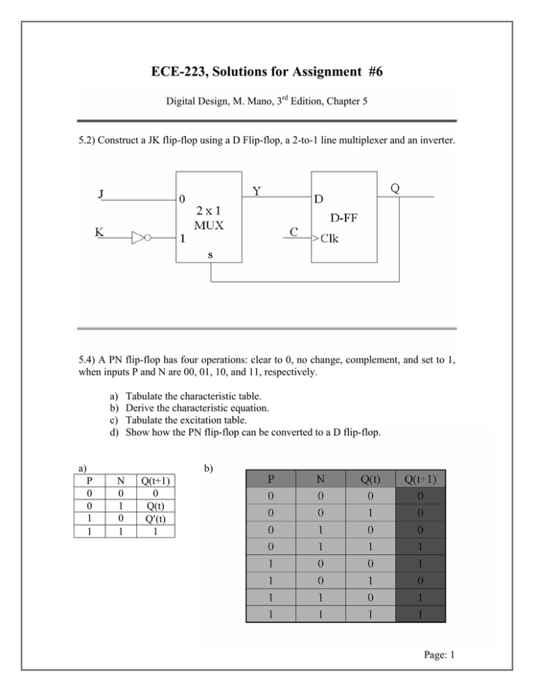
ECE-223, Solutions for Assignment #6 Digital Design, M. Mano, 3rd Edition, Chapter 5 5.2) Construct a JK flip-flop using a D Flip-flop, a 2-to-1 line multiplexer and an inverter. 5.4) A PN flip-flop has four operations: clear to 0, no change, complement, and set to 1, when inputs P and N are 00, 01, 10, and 11, respectively. a) b) c) d) a) P 0 0 1 1 Tabulate the characteristic table. Derive the characteristic equation. Tabulate the excitation table. Show how the PN flip-flop can be converted to a D flip-flop. b) N 0 1 0 1 Q(t+1) 0 Q(t) Q′(t) 1 Page: 1 Q(t+1) = PQ′ + NQ c) Q(t) 0 0 1 1 Q(t+1) 0 1 0 1 P 0 1 X X N X X 0 1 d) By connecting P and N together. Q(t+1) = DQ′ + DQ = D 5.6) A sequential circuit with two D Flip-Flops, A and B; two inputs, x and y; and one output, z, is specified by the following next-state and output equations: A(t+1) = x′y + xA B(t+1) = x′B + xA z=B a) Draw the logic diagram of the circuit. b) List the state table for the sequential circuit. c) Draw the corresponding state diagram. a) Page: 2 b) Present State A B 0 0 0 0 0 0 0 0 0 1 0 1 0 1 0 1 1 0 1 0 1 0 1 0 1 1 1 1 1 1 1 1 Inputs x 0 0 1 1 0 0 1 1 0 0 1 1 0 0 1 1 y 0 1 0 1 0 1 0 1 0 1 0 1 0 1 0 1 Next State A B 0 0 1 0 0 0 0 0 0 1 1 1 0 0 0 0 0 0 1 0 1 1 1 1 0 1 1 1 1 1 1 1 Output z 0 0 0 0 1 1 1 1 0 0 0 0 1 1 1 1 c) Page: 3 5.12) Reduce the number of states in the following state table and tabulate the reduced state table. Present State a b c d e f g h x =0 f d f g d f g g Next State Present State a b d f g x =0 f d g f g Output x =1 b c e a c b h a x =0 0 0 0 1 0 1 0 1 x =1 b a a b d x =0 0 0 1 1 0 Next State x =1 0 0 0 0 0 1 1 0 Output x =1 0 0 0 1 1 5-16) Design a sequential circuit with two D Flip-Flops, A and B, and one input x. When x = 0, then the state of the circuit remains the same. When x =1, the circuit goes through the state transitions from 00 to 01 to 11 to 10 back to 00, and repeats. Present State AB 00 00 01 01 10 10 11 11 Input x 0 1 0 1 0 1 0 1 Nest State AB 00 01 01 11 10 00 11 10 Page: 4 5-17) Design a one input, one output serial 2’s complimenter. The circuit accepts a string of bits from the input and generates the 2’s compliment at the output. The circuit can be reset asynchronously to start and end the operation. Solution: The output is 0 for all 0 inputs until the first 1 occurs at which time, the output is 1. Thereafter, the output is the complement of the input. Page: 5 The state diagram has two states State 0 : Output = Input State1 : Output = Complement of input PS A 0 0 1 1 Inp. NS Out x A y 0 0 0 1 1 1 0 1 1 1 1 0 DA= A + x y=A⊕x Page: 6 5-19) A sequential circuit has three flip-flops A, B, C; one input x; and one output, y. The state diagram is shown in Fig.P5-19. The circuit is to be designed by treating the unused states as don’t-care conditions. Analyze the circuit obtained from the design to determine the effect of the unused states. a) Use D flip-flops in the design b) Use J-K flip-flops in the design Fig.P5-19 Page: 7 a) A 0 0 0 0 0 0 0 0 1 1 Present State B 0 0 0 0 1 1 1 1 0 0 C 0 0 1 1 0 0 1 1 0 0 Input x 0 1 0 1 0 1 0 1 0 1 A 0 1 0 1 0 0 0 0 0 0 Next State B 1 0 0 0 1 0 0 1 1 1 C 1 0 1 0 0 0 1 0 0 1 Output y 0 1 0 1 0 1 0 1 0 0 Page: 8 b) Use JK flip-flops: JA 0 1 0 1 0 0 0 0 X X JA = B′x KA =1 KA X X X X X X X X 1 1 JB = A+ C′x′ KB =C′x + Cx′ JB 1 0 0 0 X X X X 1 1 KB X X X X 0 1 1 0 X X JC 1 0 X X 0 0 X X 0 1 KC X X 0 1 X X 0 1 X X JC = Ax + A′B′x′ KC =x Self-correction because KA =1 Page: 9 5-20) Design the sequential circuit specified by the state diagram of Fig. 5-19 using T flip-flops. Fig. 5-19 From State table (Table 5-4 from Digital Design, M. Mano, 3rd Edition, pp.186) TA (A, B, x) = ∑ ( 2, 3, 6) TB (A, B, x) = ∑ ( 0, 3, 4, 6) TB = A′B+Bx′ TA = Ax′+B′x′+A′Bx Page: 10


