[ /Title
(AN96
09)
/Subje
ct
(Overc
oming
Comm
on
Mode
Range
Issues
When
Using
Intersil
Integr
ating
Conve
rters)
/Autho
r ()
/Keyw
ords
(Inters
il
Corpo
ration,
semic
onduc
tor)
/Creat
or ()
/DOCI
NFO
pdfma
rk
Overcoming Common Mode Range Issues When
Using Intersil Integrating Converters
®
Application Note
August 30, 2006
AN9609.3
Authors: Paul Traynham and Juan C. Garcia
Introduction
Some applications which utilize Intersil’s integrating analog
to digital converters may require a way to overcome Common Mode Range (CMR) issues that may arise. Intersil’s
integrating analog to digital converters such as those listed
in Table 1 operate consistently with an input which is within
the CMR and the full-scale voltage set by the user. As a
result, the converter’s full scale range may vary from 200mV
to as much as 2V.
TABLE 1. INTERSIL INTEGRATING CONVERTERS
ICL7106
ICL7107
ICL7136
TO PIN 1
ICL7107
OSC 1 40
OSC 2 39
100K
OSC 3 38
TEST 37
100pF
REF HI 36
REF LO 35
CREF 34
CREF 33
31/2 Digit LCD Display ADC
31/2 Digit LED Display ADC
31/2 Digit LCD Low Power Display ADC with
SET VREF
TO 100mV
+5V
1K
10K
15K
0.1µF
1.2V (ICL8069)
COMMON 32
+
IN HI 31
Overrange Recovery
A-Z 29
Applications
BUFF 28
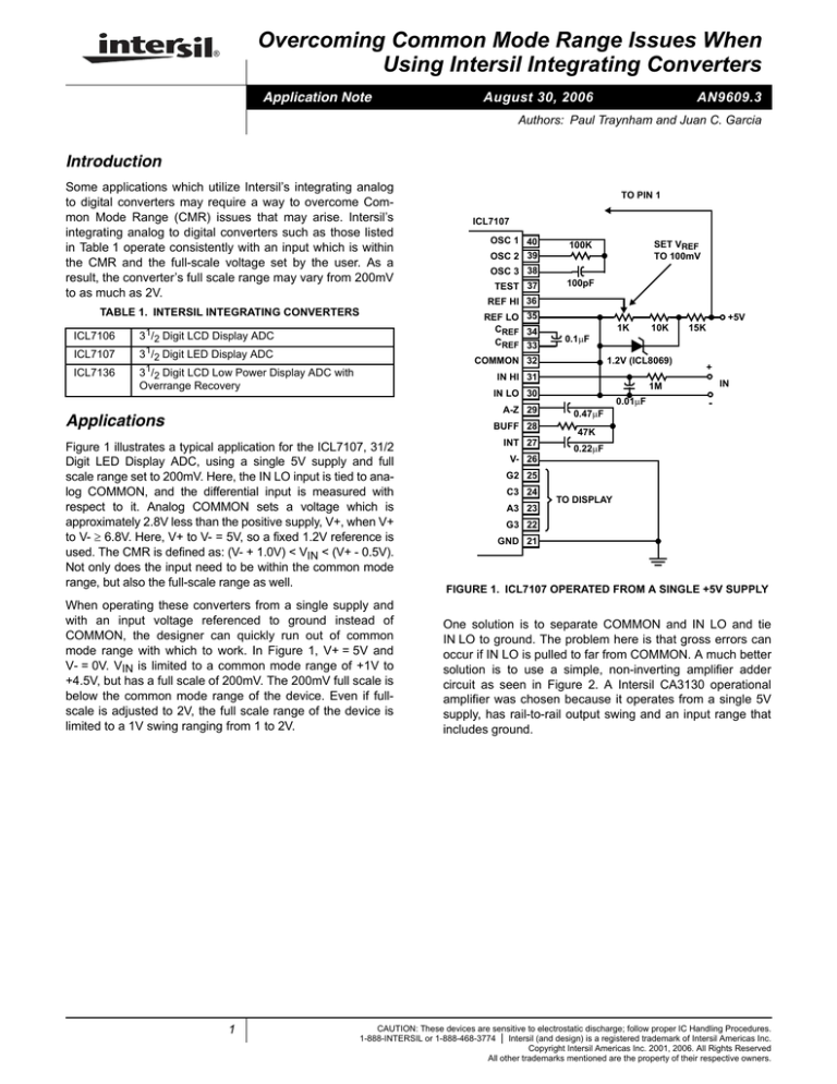
Figure 1 illustrates a typical application for the ICL7107, 31/2
Digit LED Display ADC, using a single 5V supply and full
scale range set to 200mV. Here, the IN LO input is tied to analog COMMON, and the differential input is measured with
respect to it. Analog COMMON sets a voltage which is
approximately 2.8V less than the positive supply, V+, when V+
to V- ≥ 6.8V. Here, V+ to V- = 5V, so a fixed 1.2V reference is
used. The CMR is defined as: (V- + 1.0V) < VIN < (V+ - 0.5V).
Not only does the input need to be within the common mode
range, but also the full-scale range as well.
When operating these converters from a single supply and
with an input voltage referenced to ground instead of
COMMON, the designer can quickly run out of common
mode range with which to work. In Figure 1, V+ = 5V and
V- = 0V. VIN is limited to a common mode range of +1V to
+4.5V, but has a full scale of 200mV. The 200mV full scale is
below the common mode range of the device. Even if fullscale is adjusted to 2V, the full scale range of the device is
limited to a 1V swing ranging from 1 to 2V.
INT 27
IN
1M
IN LO 30
0.01µF
-
0.47µF
47K
0.22µF
V- 26
G2 25
C3 24
A3 23
TO DISPLAY
G3 22
GND 21
FIGURE 1. ICL7107 OPERATED FROM A SINGLE +5V SUPPLY
One solution is to separate COMMON and IN LO and tie
IN LO to ground. The problem here is that gross errors can
occur if IN LO is pulled to far from COMMON. A much better
solution is to use a simple, non-inverting amplifier adder
circuit as seen in Figure 2. A Intersil CA3130 operational
amplifier was chosen because it operates from a single 5V
supply, has rail-to-rail output swing and an input range that
includes ground.
[
/Page
1
CAUTION: These devices are sensitive to electrostatic discharge; follow proper IC Handling Procedures.
1-888-INTERSIL or 1-888-468-3774 | Intersil (and design) is a registered trademark of Intersil Americas Inc.
Copyright Intersil Americas Inc. 2001, 2006. All Rights Reserved
All other trademarks mentioned are the property of their respective owners.
Application Note 9609
Measuring the Supply Rail
TO PIN 1
ICL7107
In battery applications where a designer wishes to not only
power the converter from a single supply, but also monitor
and display the battery voltage, common mode range issues
again arise. From the CMR equation we note that:
SET VREF
100K
OSC 2 39
TO 100mV
OSC 3 38
1V < VIN < (V+ - 0.5V)
100pF
REF HI 36
REF LO 35
CREF 34
CREF 33
At first glance, it may seem that an easy solution would be to
use a simple resistor voltage divider and reduce VIN by a
factor of 10, set full-scale to 2V and supply this to the ADC.
For common battery voltages of 6V to 12V, the
corresponding input voltages would be 0.6 to 1.2V. However,
if we go back to the above common mode range equation, it
states that VIN must be greater than 1V. Figure 3 illustrates
another operational amplifier configuration to solve this
problem. Again a CA3130 was chosen because of its
characteristics.
+5V
1K
15K
10K
0.1µF
1.2V (ICL8069)
COMMON 32
IN HI 31
1M
IN LO 30
INT 27
0.47µF
CA3130
R
-
BUFF 28
Rf
0.01µF
47K
VOUT
0.22µF
+
A-Z 29
VCOM
V- 26
TO PIN 1
VIN′
ICL7106
VIN
G2 25
R1
R1
C3 24
TO DISPLAY
OSC 1 40
OSC 2 39
A3 23
OSC 3 38
TEST 37
G3 22
REF HI 36
GND 21
REF LO 35
CREF 34
CREF 33
100pF
25K
-
9V
IN HI 31
IN LO 30
By analyzing the circuit in Figure 2, we see that:
A-Z 29
(EQ. 1)
BUFF 28
INT 27
0.01µF
0.47µF
0.22µF
C3 24
A3 23
R
CA3130
VOUT
VIN
VIN′
VCOM
G2 25
(EQ. 2)
Rf
470K
V- 26
where
1
V IN ′ = --- ( V IN + V COM )
2
+
25K
0.1µF
COMMON 32
FIGURE 2. SIMPLE SUMMING AMP TO RESOLVE CMR
PROBLEM
R
V OUT = ⎛ 1 + ------f⎞ × V IN ′
⎝
R⎠
SET VREF
TO 1V
100K
+
TEST 37
-
OSC 1 40
R1
R2
TO DISPLAY
G3 22
to define the operational amplifier output.
BP 21
TO BACKPLANE
Substituting equation 2 into equation 1, and setting Rf = R
yields:
1
V OUT = 2 ⎛ --- ( V IN + V COM )⎞ = V IN + V COM
⎝2
⎠
(EQ. 3)
Using this circuit, the operational amplifier’s output signal
(VOUT) is now the sum of the incoming signal (VIN) and
COMMON. In other words, VIN is now referenced with
respect to COMMON and not ground. With a single 5V
supply, an external voltage reference must be used because
the internal reference is only active when V+ to V- ≥ 6.8V,
and VCOM = COMMON ≅ V+ - 1.2V = 3.8V. The signal input
to the ICL7107 will now be offset by 3.8V, which is well within
the common mode range of the device. Even if V+ changes,
as in battery applications, COMMON will keep the signal
within the common mode range of the converter.
2
FIGURE 3. SIMPLE OP AMP CIRCUIT TO MEASURE SUPPLY
RAIL (V+)
Here an ICL7106, 31/2 Digit LCD Display ADC with full scale
set to 2V is shown. In this circuit, the operational amplifier is
set in an inverting gain configuration, because gains of 0.1
are desirable, and because we are only concerned with positive input voltages.
AN9609.3
August 30, 2006
Application Note 9609
Again analyzing the operational amplifier configuration, we
note that:
( V IN ′ – V IN )
( V OUT – V IN ′ )
-------------------------------- = -------------------------------------R
RF
For more information on Intersil integrating analog to digital
converters, please refer to the following data sheets:
(EQ. 4)
TABLE 2
DEVICE
and that:
⎛ R2 ⎞
V IN ′ = V COM ⎜ ---------------------⎟
⎝ R 1 + R 2⎠
ICL7106
31/2 Digit LCD/LED Display ADC
ICL7107
31/2 Digit LCD/LED Display ADC
ICL7136
31/2 Digit LCD/LED Low Power Display ADC with
Overrange Recovery
(EQ. 5)
Setting R = 10RF, RF = R1 and R2 = 10R1, the equations
can be reduced to:
V IN ′ – V IN = 10 ( V OUT – V IN ′ )
DESCRIPTION
(EQ. 6)
and
10V COM
⎛ ( 10 × V COM × R 1 )⎞
V IN ′ = ⎜ ------------------------------------------------⎟ = ----------------------11R
11
⎝
⎠
1
(EQ. 7)
Combining equations 6 and 7 reveals that:
V IN
V OUT = V COM – --------10
(EQ. 8)
The output of the operational amplifier (VOUT), which is the
input of the ADC, is now -0.1VIN with respect to COMMON,
and since VIN = V+, the ADC will measure -10% of the supply. Simply driving the proper decimal point and not driving
the sign indicator will display the proper voltage. For example, a battery voltage of 11.6V will be measured as -1.16V
and can easily be displayed as 11.60V on a 31/2 Digit
Display.
All Intersil U.S. products are manufactured, assembled and tested utilizing ISO9000 quality systems.
Intersil Corporation’s quality certifications can be viewed at www.intersil.com/design/quality
Intersil products are sold by description only. Intersil Corporation reserves the right to make changes in circuit design, software and/or specifications at any time without
notice. Accordingly, the reader is cautioned to verify that data sheets are current before placing orders. Information furnished by Intersil is believed to be accurate and
reliable. However, no responsibility is assumed by Intersil or its subsidiaries for its use; nor for any infringements of patents or other rights of third parties which may result
from its use. No license is granted by implication or otherwise under any patent or patent rights of Intersil or its subsidiaries.
For information regarding Intersil Corporation and its products, see www.intersil.com
3
AN9609.3
August 30, 2006
