DATASHEET
IDT5T30553
LOW SKEW 1 TO 4 CLOCK BUFFER
Description
Features
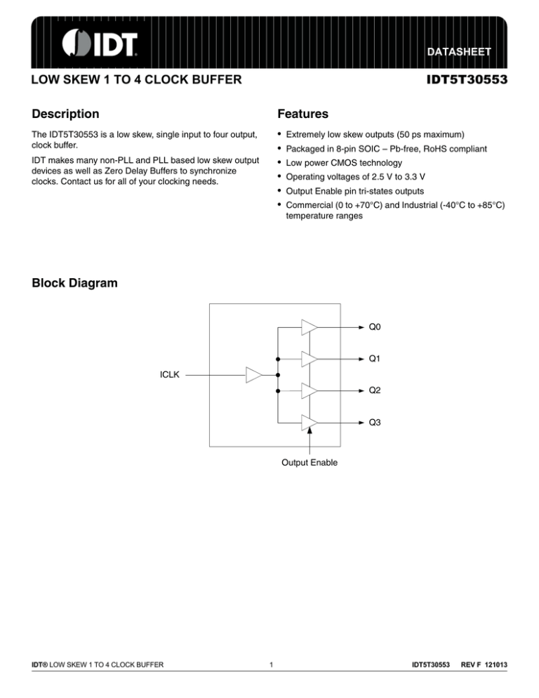
The IDT5T30553 is a low skew, single input to four output,
clock buffer.
•
•
•
•
•
•
IDT makes many non-PLL and PLL based low skew output
devices as well as Zero Delay Buffers to synchronize
clocks. Contact us for all of your clocking needs.
Extremely low skew outputs (50 ps maximum)
Packaged in 8-pin SOIC – Pb-free, RoHS compliant
Low power CMOS technology
Operating voltages of 2.5 V to 3.3 V
Output Enable pin tri-states outputs
Commercial (0 to +70°C) and Industrial (-40°C to +85°C)
temperature ranges
Block Diagram
Q0
Q1
ICLK
Q2
Q3
Output Enable
IDT® LOW SKEW 1 TO 4 CLOCK BUFFER
1
IDT5T30553
REV F 121013
IDT5T30553
LOW SKEW 1 TO 4 CLOCK BUFFER
FAN OUT BUFFER
Pin Assignment
VDD
1
8
OE
Q0
2
7
Q3
Q1
3
6
Q2
GN D
4
5
I CL K
8 - p i n S OI C
Pin Descriptions
Pin
Pin
Number Name
Pin
Type
Pin Description
1
VDD
Power
Connect to +2.5 V or +3.3 V.
2
Q0
Output
Clock output 0.
3
Q1
Output
Clock output 1.
4
GND
Power
Connect to ground.
5
ICLK
Input
Clock input.
6
Q2
Output
Clock Output 2.
7
Q3
Output
Clock Output 3.
8
OE
Input
Output Enable. Tri-states outputs when low. Connect to VDD for normal operation.
External Components
A minimum number of external components are required for proper operation. A decoupling capacitor of 0.01 µF
should be connected between VDD on pin 1 and GND on pin 4, as close to the device as possible. A 33 series
terminating resistor may be used on each clock output if the trace is longer than 1 inch.
To achieve the low output skew that the IDT5T30553 is capable of, careful attention must be paid to board layout.
Essentially, all four outputs must have identical terminations, identical loads and identical trace geometries. If they
do not, the output skew will be degraded. For example, using a 30 series termination on one output (with 33 on
the others) will cause at least 15 ps of skew.
IDT® LOW SKEW 1 TO 4 CLOCK BUFFER
2
IDT5T30553
REV F 121013
IDT5T30553
LOW SKEW 1 TO 4 CLOCK BUFFER
FAN OUT BUFFER
Absolute Maximum Ratings
Stresses above the ratings listed below can cause permanent damage to the IDT5T30553. These ratings, which
are standard values for IDT commercially rated parts, are stress ratings only. Functional operation of the device at
these or any other conditions above those indicated in the operational sections of the specifications is not implied.
Exposure to absolute maximum rating conditions for extended periods can affect product reliability. Electrical
parameters are guaranteed only over the recommended operating temperature range.
Item
Rating
Supply Voltage, VDD
7V
Output Enable and All Outputs
-0.5V to VDD+0.5 V
ICLK
-0.5V to VDD+0.5V
Ambient Operating Temperature (industrial)
-40C to +85C
Storage Temperature
-65C to +150C
Junction Temperature
125C
Soldering Temperature
260C
Recommended Operation Conditions
Parameter
Min.
Max.
Units
-40
+85
C
+2.375
+3.465
V
Ambient Operating Temperature (industrial)
Power Supply Voltage (measured in respect to GND)
Typ.
DC Electrical Characteristics
VDD=2.5 V ±5%, Ambient temperature -40 to +85C, unless stated otherwise
Parameter
Operating Voltage
Symbol
Conditions
Min.
Typ.
Max.
Units
VDD
2.375
2.625
V
Input High Voltage, OE
VIH
1.8
VDD
V
Input Low Voltage, OE
VIL
0.7
V
Output High Voltage
VOH
IOH = -16 mA
Output Low Voltage
VOL
IOL = 16 mA
Operating Supply Current
IDD
No load, 135 MHz
Nominal Output Impedance
ZO
Input Capacitance
CIN
Short Circuit Current
IOS
IDT® LOW SKEW 1 TO 4 CLOCK BUFFER
ICLK, OE pin
3
2
V
0.4
V
25
mA
20
5
pF
±28
mA
IDT5T30553
REV F 121013
IDT5T30553
LOW SKEW 1 TO 4 CLOCK BUFFER
FAN OUT BUFFER
DC Electrical Characteristics (continued)
VDD=3.3 V ±5% , Ambient temperature -40 to +85C, unless stated otherwise
Parameter
Symbol
Operating Voltage
Conditions
Min.
Typ.
Max.
Units
VDD
3.135
3.465
V
Input High Voltage, OE
VIH
2
VDD
V
Input Low Voltage, OE
VIL
0.8
V
Output High Voltage
VOH
IOH = -25 mA
Output Low Voltage
VOL
IOL = 25 mA
Output High Voltage (CMOS
Level)
VOH
IOH = -12 mA
Operating Supply Current
IDD
No load, 135 MHz
Nominal Output Impedance
ZO
Input Capacitance
CIN
Short Circuit Current
IOS
2.4
V
0.4
V
VDD-0.4
V
ICLK, OE pin
35
mA
20
5
pF
±50
mA
Notes: 1. Nominal switching threshold is VDD/2
AC Electrical Characteristics
VDD = 2.5 V ±5%, Ambient Temperature -40 to +85C, unless stated otherwise
Parameter
Symbol
Conditions
Input Frequency
Min.
Typ.
0
Max. Units
200
MHz
Output Rise Time
tOR
0.8 to 2.0 V, CL=15 pF
1.0
1.5
ns
Output Fall Time
tOF
2.0 to 0.8 V, CL=15 pF
1.0
1.5
ns
1
ps
3
5
ns
0
50
ps
500
ps
Additive Period Jitter
Propagation Delay
Note 1
Output to Output Skew
Note 2
Device to Device Skew
2.2
Rising edges at VDD/2
Rising edges at VDD/2
VDD = 3.3 V ±5%, Ambient Temperature -40 to +85C, unless stated otherwise
Parameter
Symbol
Conditions
Input Frequency
Min.
Typ.
0
Max. Units
200
MHz
Output Rise Time
tOR
0.8 to 2.0 V, CL=15 pF
0.6
1.0
ns
Output Fall Time
tOF
2.0 to 0.8 V, CL=15 pF
0.6
1.0
ns
2.4
4
ns
1
ps
50
ps
500
ps
Propagation Delay
Note 1
2.0
Additive Period Jitter
Output to Output Skew
Device to Device Skew
Note 2
Rising edges at VDD/2
Rising edges at VDD/2
0
Notes: 1. With rail to rail input clock.
2. Between any 2 outputs with equal loading.
3. Duty cycle on outputs will match incoming clock duty cycle. Consult IDT for tight duty cycle clock
generators.
IDT® LOW SKEW 1 TO 4 CLOCK BUFFER
4
IDT5T30553
REV F 121013
IDT5T30553
LOW SKEW 1 TO 4 CLOCK BUFFER
FAN OUT BUFFER
Thermal Characteristics
Parameter
Symbol
Thermal Resistance Junction to
Ambient
Conditions
Min.
Max. Units
JA
Still air
150
C/W
JA
1 m/s air flow
140
C/W
JA
3 m/s air flow
120
C/W
40
C/W
JC
Thermal Resistance Junction to Case
Typ.
Marking Diagrams
8
5
8
IDT5T30
553DCG
YYWW$
1
5
IDT5T30
553DCGI
YYWW$
4
1
4
Notes:
1. “$” is the mark code.
2. YYWW is the last two digits of the year and week that the part was assembled.
3 “G” after the two-letter package code denotes RoHS compliant package.
4. “I” denotes industrial temperature range device.
5. Bottom marking: country of origin.
IDT® LOW SKEW 1 TO 4 CLOCK BUFFER
5
IDT5T30553
REV F 121013
IDT5T30553
LOW SKEW 1 TO 4 CLOCK BUFFER
FAN OUT BUFFER
Package Outline and Package Dimensions (8-pin SOIC, 150 Mil. Narrow Body)
Package dimensions are kept current with JEDEC Publication No. 95
Millimeters
Symbol
Min
Max
Min
Max
A
1.35
1.75
.0532
.0688
A1
0.10
0.25
.0040
.0098
B
0.33
0.51
.013
.020
C
0.19
0.25
.0075
.0098
D
4.80
5.00
.1890
.1968
E
3.80
4.00
.1497
.1574
8
E
Inches*
H
INDEX
AREA
e
1 2
D
1.27 BASIC
0.050 BASIC
H
5.80
6.20
.2284
.2440
h
0.25
0.50
.010
.020
L
0.40
1.27
.016
.050
0
8
0
8
*For reference only. Controlling dimensions in mm.
A
h x 45
A1
C
-Ce
SEATING
PLANE
B
L
.10 (.004)
C
Ordering Information
Part / Order Number
Marking
Shipping Packaging
Package
Temperature
5T30553DCG
5T30553DCG8
5T30553DCGI
5T30553DCGI8
see page 6
Tubes
Tape and Reel
Tubes
Tape and Reel
8-pin SOIC
8-pin SOIC
8-pin SOIC
8-pin SOIC
0 to +70 C
0 to +70 C
-40 to +85 C
-40 to +85 C
“G” after the two-letter package code denotes Pb-Free configuration, RoHS compliant.
While the information presented herein has been checked for both accuracy and reliability, Integrated Device Technology (IDT) result from
its use. No other circuits, patents, or licenses are implied. This product is intended for use in normal commercial applications. Any other
applications such as those requiring extended temperature range, high reliability, or other extraordinary environmental requirements are
not recommended without additional processing by IDT. IDT reserves the right to change any circuitry or specifications without notice. IDT
does not authorize or warrant any IDT product for use in life support devices or critical medical instruments.
IDT® LOW SKEW 1 TO 4 CLOCK BUFFER
6
IDT5T30553
REV F 121013
IDT5T30553
LOW SKEW 1 TO 4 CLOCK BUFFER
FAN OUT BUFFER
Revision History
Rev.
Originator
Date
Description of Change
B
P. Keyashian
02/17/09
Added industrial temp ordering information.
C
P. Keyashian
09/02/09
Added “Additive Period Jitter” spec.
D
V. Chaudry
03/22/12
Added marking diagrams and notes
E
A. Tsui
06/21/12
Change Operating Voltage specs from 3.15V Min/3.45V Max to 3.135V Min/3.465V Max
F
S. Sharma
12/10/13
Updated max rating for ICLK voltage to be “-0.5V to VDD+0.5V”
IDT® LOW SKEW 1 TO 4 CLOCK BUFFER
7
IDT5T30553
REV F 121013
IDT5T30553
LOW SKEW 1 TO 4 CLOCK BUFFER
FAN OUT BUFFER
Innovate with IDT and accelerate your future networks. Contact:
www.IDT.com
For Sales
For Tech Support
800-345-7015
408-284-8200
Fax: 408-284-2775
www.idt.com/go/clockhelp
Corporate Headquarters
Integrated Device Technology, Inc.
www.idt.com
© 2013 Integrated Device Technology, Inc. All rights reserved. Product specifications subject to change without notice. IDT and the IDT logo are trademarks of Integrated Device
Technology, Inc. Accelerated Thinking is a service mark of Integrated Device Technology, Inc. All other brands, product names and marks are or may be trademarks or registered
trademarks used to identify products or services of their respective owners.
Printed in USA
