DATASHEET
ICS574
ZERO DELAY, LOW SKEW BUFFER
Description
Features
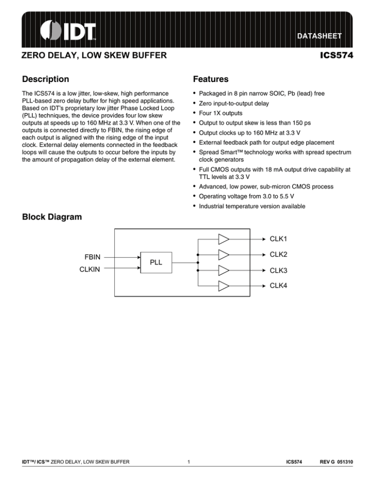
The ICS574 is a low jitter, low-skew, high performance
PLL-based zero delay buffer for high speed applications.
Based on IDT’s proprietary low jitter Phase Locked Loop
(PLL) techniques, the device provides four low skew
outputs at speeds up to 160 MHz at 3.3 V. When one of the
outputs is connected directly to FBIN, the rising edge of
each output is aligned with the rising edge of the input
clock. External delay elements connected in the feedback
loops will cause the outputs to occur before the inputs by
the amount of propagation delay of the external element.
•
•
•
•
•
•
•
Packaged in 8 pin narrow SOIC, Pb (lead) free
Zero input-to-output delay
Four 1X outputs
Output to output skew is less than 150 ps
Output clocks up to 160 MHz at 3.3 V
External feedback path for output edge placement
Spread Smart™ technology works with spread spectrum
clock generators
• Full CMOS outputs with 18 mA output drive capability at
TTL levels at 3.3 V
• Advanced, low power, sub-micron CMOS process
• Operating voltage from 3.0 to 5.5 V
• Industrial temperature version available
Block Diagram
CLK1
FBIN
CLKIN
CLK2
PLL
CLK3
CLK4
IDT™/ ICS™ ZERO DELAY, LOW SKEW BUFFER
1
ICS574
REV G 051310
ICS574
ZERO DELAY, LOW SKEW BUFFER
ZDB
Pin Assignment
CLKIN
1
8
FBIN
CLK1
2
7
CLK4
CLK2
3
6
CLK3
GND
4
5
VDD
Pin Descriptions
Pin
Number
Pin
Name
Pin
Type
1
CLKIN
Input
2, 3, 6, 7
CLK1:4
Output
Clock Outputs (4).
4
GND
Power
Connect to ground.
5
VDD
Power
Power supply. Connect both pins to same voltage (either 3.3 V or 5 V).
8
FBIN
Input
Feedback input.
IDT™/ ICS™ ZERO DELAY, LOW SKEW BUFFER
Pin Description
Clock input. Connect to input clock source.
2
ICS574
REV G 051310
ICS574
ZERO DELAY, LOW SKEW BUFFER
ZDB
External Components
The ICS574 requires a minimum number of external components for proper operation. Decoupling capacitors of
0.1µF should be connected between VDD and GND on pins 4 and 5, as close to the device as possible. A series
termination resistor of 33Ω may be used close to the pin for each clock output to reduce reflections.
Absolute Maximum Ratings
Stresses above the ratings listed below can cause permanent damage to the ICS574. These ratings, which are
standard values for IDT commercially rated parts, are stress ratings only. Functional operation of the device at these
or any other conditions above those indicated in the operational sections of the specifications is not implied.
Exposure to absolute maximum rating conditions for extended periods can affect product reliability. Electrical
parameters are guaranteed only over the recommended operating temperature range.
Item
Rating
Supply Voltage, VDD (referenced to ground)
-0.5 V to 7 V
All Inputs and Outputs
-0.5 V to VDD+0.5 V
Electrostatic Discharge (MIl-STD-883)
2000 V (minimum)
Ambient Operating Temperature
-40° C to +85° C
Soldering Temperature (10 seconds max.)
260° C
Junction Temperature
150° C
Storage Temperature
-65 to +150° C
IDT™/ ICS™ ZERO DELAY, LOW SKEW BUFFER
3
ICS574
REV G 051310
ICS574
ZERO DELAY, LOW SKEW BUFFER
ZDB
DC Electrical Characteristics
Unless stated otherwise, VDD = 3.3 V, Ambient Temperature -40 to +85° C
Parameter
Symbol
Operating Supply Voltage
Conditions
Min.
Typ.
Max.
Units
5.5
V
VDD
3
Input High Voltage
VIH
VDD/2+1
Input Low Voltage
VIL
Output High Voltage, CMOS
level
VOH
IOH = -5 mA
VDD-0.4
V
Output High Voltage
VOH
IOH = -18 mA
2.4
V
Output Low Voltage
VOL
IOL = 18 mA
IDD Operating Supply Current
Short Circuit Current
IOS
Input Capacitance
CIN
V
VDD/2-1
0.4
V
V
No load (Note 2)
36
mA
Each output
±65
mA
7
pF
AC Electrical Characteristics
Unless stated otherwise, VDD = 3.3 V, Ambient Temperature -40 to +85° C
Parameter
Input Frequency, clock
Symbol
fIN
Conditions
Min.
Typ.
Max. Units
FBIN from CLK4
20
160
MHz
Output Frequency, clock
FBIN from CLK4
20
160
MHz
Output Clock Rise Time
0.8 to 2.0 V, 15 pF load
1.5
ns
Output Clock Fall Time
2.0 to 0.8 V, 15 pF load
1.5
ns
Output Clock Duty Cycle, 3.3 V
At 1.4 V
60
%
Device-to-device Skew, equally
loaded
Rising edges at VDD/2
700
ps
Outpu-to-output Skew, equally
loaded
Rising edges at VDD/2
150
ps
Maximum Absolute Jitter
Cycle-to-cycle Jitter, 15 pF loads
40
50
170
66.67 MHz outputs
ps
250
ps
Notes:
1. Stresses beyond those listed in Absolute Maximum Ratings can permanently damage the device. Prolonged
exposure to levels above the operating limits but below the Absolute Maximum Ratings may affect device reliability.
2. With CLKIN = 160 MHz, FBIN to CLK4.
Using Spread Spectrum Input Clocks
The ICS574 uses IDT’s Spread Smart technology, allowing it to accurately track (pass through) any clocks that
implement spread spectrum techniques.
IDT™/ ICS™ ZERO DELAY, LOW SKEW BUFFER
4
ICS574
REV G 051310
ICS574
ZERO DELAY, LOW SKEW BUFFER
ZDB
Thermal Characteristics
Parameter
Thermal Resistance Junction to
Ambient
Symbol
Min.
Typ.
Max. Units
θJA
Still air
150
° C/W
θJA
1 m/s air flow
140
° C/W
θJA
3 m/s air flow
120
° C/W
40
° C/W
20
° C/W
Thermal Resistance Junction to Case
θJC
Thermal Resistance Junction to Top
of Case
ΨJT
IDT™/ ICS™ ZERO DELAY, LOW SKEW BUFFER
Conditions
Still air
5
ICS574
REV G 051310
ICS574
ZERO DELAY, LOW SKEW BUFFER
ZDB
Package Outline and Package Dimensions (8-pin SOIC, 150 Mil. Body)
Package dimensions are kept current with JEDEC Publication No. 95
8
Millimeters
Symbol
E
Min
A
A1
B
C
D
E
e
H
h
L
α
H
INDEX
AREA
1 2
D
A
Inches
Max
Min
1.35
1.75
0.10
0.25
0.33
0.51
0.19
0.25
4.80
5.00
3.80
4.00
1.27 BASIC
5.80
6.20
0.25
0.50
0.40
1.27
0°
8°
Max
.0532
.0688
.0040
.0098
.013
.020
.0075
.0098
.1890
.1968
.1497
.1574
0.050 BASIC
.2284
.2440
.010
.020
.016
.050
0°
8°
h x 45
A1
C
-Ce
B
SEATING
PLANE
L
.10 (.004)
C
Ordering Information
Part / Order Number
Marking
Shipping Packaging
Package
Temperature
574MLF
574MLFT
574MILF
574MILFT
574MLF
Tubes
Tape and Reel
Tubes
Tape and Reel
8-pin SOIC
8-pin SOIC
8-pin SOIC
8-pin SOIC
0 to +70° C
0 to +70° C
-40 to +85° C
-40 to +85° C
574MILF
"LF" suffix to the part number are the Pb-Free configuration and are RoHS compliant.
While the information presented herein has been checked for both accuracy and reliability, Integrated Device Technology (IDT) assumes
no responsibility for either its use or for the infringement of any patents or other rights of third parties, which would result from its use. No
other circuits, patents, or licenses are implied. This product is intended for use in normal commercial applications. Any other applications
such as those requiring extended temperature range, high reliability, or other extraordinary environmental requirements are not
recommended without additional processing by IDT. IDT reserves the right to change any circuitry or specifications without notice. IDT
does not authorize or warrant any IDT product for use in life support devices or critical medical instruments.
IDT™/ ICS™ ZERO DELAY, LOW SKEW BUFFER
6
ICS574
REV G 051310
ICS574
ZERO DELAY, LOW SKEW BUFFER
ZDB
Innovate with IDT and accelerate your future networks. Contact:
www.IDT.com
For Sales
For Tech Support
800-345-7015
408-284-8200
Fax: 408-284-2775
www.idt.com/go/clockhelp
Corporate Headquarters
Integrated Device Technology, Inc.
www.idt.com
© 2006 Integrated Device Technology, Inc. All rights reserved. Product specifications subject to change without notice. IDT and the IDT logo are trademarks of Integrated Device
Technology, Inc. Accelerated Thinking is a service mark of Integrated Device Technology, Inc. All other brands, product names and marks are or may be trademarks or registered
trademarks used to identify products or services of their respective owners.
Printed in USA
