MPQ2451-5/33
36V, 2.2MHz, 0.6A, Step-Down Converter
AEC-Q100 Qualified
DESCRIPTION
FEATURES
The MPQ2451-5/33 is a high-frequency, stepdown, switching regulator with an integrated,
high-voltage, high-side power MOSFET. It
efficiently outputs up to 0.6A, with current-mode
control for fast loop response.
•
The wide 3.3V-to-36V input range accommodates
a variety of automotive step-down applications,
and the 3μA shutdown-mode quiescent current
allows use in battery-powered applications.
The MPQ2451-5/33 achieves high powerconversion efficiency over a wide load range by
scaling down the switching frequency under
light-load conditions to reduce switching and
gate driving losses.
Frequency fold-back prevents inductor current
runaway during start-up. Thermal shutdown
provides reliable, fault-tolerant operation.
The MPQ2451-5/33 is available in cost-effective
SOT23-6L and QFN-6L packages.
•
•
•
•
•
•
•
•
•
•
•
•
Guaranteed Industrial/Automotive Temp.
Ranges
130μA Operating Quiescent Current
Wide 3.3V-to-36V Operating Input Range
500mΩ Internal Power MOSFET
2.2MHz Fixed Switching Frequency
Internally Compensated
Stable with Ceramic Output Capacitors
Internal Soft-Start
Precision Current Limit Without Current
Sensing Resistor
>90% Efficiency
Fixed 5V & 3.3V Outputs
6-Lead SOT23 and QFN Packages
Available in AEC-Q100 Grade 1
APPLICATIONS
•
High-Voltage Power Conversion, Including
o Automotive Systems
o Industrial Power Systems
o Distributed Power Systems
o Battery-Powered Systems
All MPS parts are lead-free and adhere to the RoHS directive. For MPS green
status, please visit MPS website under Products, Quality Assurance page.
“MPS” and “The Future of Analog IC Technology” are registered trademarks of
Monolithic Power Systems, Inc.
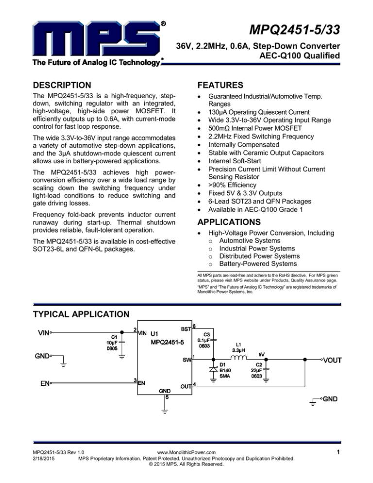
TYPICAL APPLICATION
MPQ2451-5/33 Rev 1.0
www.MonolithicPower.com
2/18/2015
MPS Proprietary Information. Patent Protected. Unauthorized Photocopy and Duplication Prohibited.
© 2015 MPS. All Rights Reserved.
1
MPQ2451-5/33―36V, 2.2MHz, 0.6A, STEP-DOWN CONVERTER, AEC-Q100 QUALIFIED
ORDERING INFORMATION
Part Number
Package
Top Marking
MPQ2451GT-5*
AGE
MPQ2451GT-5-AEC1
SOT23-6L
MPQ2451GT-33**
AGF
MPQ2451GT-33-AEC1
MPQ2451GG-5
BP
MPQ2451GG-5-AEC1
QFN-6L
MPQ2451GG-33
BQ
MPQ2451GG-33-AEC1
* For Tape & Reel, add suffix –Z (e.g. MPQ2451GT-5–AEC1-Z)
** For Tape & Reel, add suffix -Z (e.g. MPQ2451GT-33-Z)
PACKAGE REFERENCE
OUT
OUT
SOT23-6L
QFN-6L
ABSOLUTE MAXIMUM RATINGS (1)
Supply Voltage (VIN).................... −0.3V to +40V
Switch Voltage (VSW)........... −0.3V to (VIN+0.3V)
BST to SW .................................... −0.3 to +5.0V
All Other Pins ............................. –0.3V to +5.0V
(2)
Continuous Power Dissipation (TA = 25°C)
SOT23-6L ................................................0.57W
QFN-6L ....................................................1.56W
Junction Temperature .............................. 150°C
Lead Temperature ................................... 260°C
Storage Temperature .............. −65°C to +150°C
Recommended Operating Conditions
(3)
Supply Voltage VIN .......................... 3.3V to 36V
Operating Junction Temp. (TJ).−40°C to +125°C
Thermal Resistance
(4)
θJA
θJC
SOT23-6L .............................. 220 .... 110 .. °C/W
QFN-6L................................... 80 ...... 16 ... °C/W
Notes:
1) Exceeding these ratings may damage the device.
2) The maximum allowable power dissipation is a function of the
maximum junction temperature TJ (MAX), the junction-toambient thermal resistance θJA, and the ambient temperature
TA. The maximum allowable continuous power dissipation at
any ambient temperature is calculated by PD (MAX) = (TJ
(MAX)-TA)/θJA. Exceeding the maximum allowable power
dissipation will cause excessive die temperature, and the
regulator will go into thermal shutdown. Internal thermal
shutdown circuitry protects the device from permanent
damage.
3) The device is not guaranteed to function outside of its
operating conditions.
4) Measured on JESD51-7, 4-layer PCB.
MPQ2451-5/33 Rev 1.0
www.MonolithicPower.com
2/18/2015
MPS Proprietary Information. Patent Protected. Unauthorized Photocopy and Duplication Prohibited.
© 2015 MPS. All Rights Reserved.
2
MPQ2451-5/33―36V, 2.2MHz, 0.6A, STEP-DOWN CONVERTER, AEC-Q100 QUALIFIED
ELECTRICAL CHARACTERISTICS
VIN = 12V, VEN = 2V, TJ= −40°C to +125°C, unless otherwise noted. Typical values are at TJ = 25°C.
Parameter
Symbol Condition
MPQ2451-5
VOUT
Output Voltage
MPQ2451-33
Upper Switch-On Resistance
Min
Typ
Max
6V < VIN < 36V
4.8
5
5.2
6V < VIN < 36V,
TJ= 25°C
4.85
5
5.15
3.3V < VIN < 36V
3.168
3.3
3.432
3.2
3.3
3.4
3.3V < VIN <
36V, TJ= 25°C
RDS(ON)
Upper Switch Leakage
Current Limit
ILIM
COMP to Current Sense
(5)
Transconductance
GCS
VBST−VSW =5V
TJ= 25°C
500
VEN = 0V, VSW =
0V
0.5
TJ= 25°C
0.75
TJ =-40°C to
+125°C
0.65
VIN UVLO, Upper Threshold
Units
V
V
mΩ
2
μA
1
A
3
A/V
2.7
3.29
V
VIN UVLO, Hysteresis
0.4
Soft-Start Time
0.5
1
ms
2.2
2.6
MHz
Oscillator Frequency
fSW
1.8
Minimum Switch-On Time
τON
Shutdown Supply Current
IS
VEN < 0.3V
Quiescent Supply Current
IQ
No load,
no switching
(5)
Thermal Shutdown
80
130
(5)
Enable Threshold, High
V
ns
1
μA
170
µA
150
VIH
Low-to-High
Enable Threshold, Hysteresis
1.35
1.5
°C
1.8
400
V
mV
Notes:
5) Derived from bench characterization, not tested in production.
MPQ2451-5/33 Rev 1.0
www.MonolithicPower.com
2/18/2015
MPS Proprietary Information. Patent Protected. Unauthorized Photocopy and Duplication Prohibited.
© 2015 MPS. All Rights Reserved.
3
MPQ2451-5/33―36V, 2.2MHz, 0.6A, STEP-DOWN CONVERTER, AEC-Q100 QUALIFIED
PIN FUNCTIONS
SOT23-6L
Pin #
QFN-6L
Pin #
Name
1
6
BST
Bootstrap. Positive power supply for the internal, floating, high-side
MOSFET driver. Connect a bypass capacitor between this pin and SW
pin.
2
5
GND
Ground. Connect the output capacitor as close to this pin as possible.
Avoid routing near high-current switch paths.
3
4
OUT
Output-Voltage Sense. Connected to the tap of an internal resistor divider
to set the output voltage.
4
3
EN
5
2
VIN
6
1
SW
Description
Enable. Pull this pin below the specified threshold to shut the chip down.
Pull it above the specified threshold to enable the chip. Float this pin to
disable the chip.
Input Supply. Supplies power to all internal control circuitry. Requires a
decoupling capacitor to ground to reduce switching spikes.
Switch Node. Output of the high-side switch. Requires a low-VF Schottky
diode connected to ground to reduce switching spikes.
MPQ2451-5/33 Rev 1.0
www.MonolithicPower.com
2/18/2015
MPS Proprietary Information. Patent Protected. Unauthorized Photocopy and Duplication Prohibited.
© 2015 MPS. All Rights Reserved.
4
MPQ2451-5/33―36V, 2.2MHz, 0.6A, STEP-DOWN CONVERTER, AEC-Q100 QUALIFIED
TYPICAL CHARACTERISTICS
MPQ2451-5/33 Rev 1.0
www.MonolithicPower.com
2/18/2015
MPS Proprietary Information. Patent Protected. Unauthorized Photocopy and Duplication Prohibited.
© 2015 MPS. All Rights Reserved.
5
MPQ2451-5/33―36V, 2.2MHz, 0.6A, STEP-DOWN CONVERTER, AEC-Q100 QUALIFIED
TYPICAL PERFORMANCE CHARACTERISTICS
VIN = 12V, C1 = 10µF, C2 = 22µF, L = 3.3µH and TA= 25°C, unless otherwise noted.
MPQ2451-5
MPQ2451-5/33 Rev 1.0
www.MonolithicPower.com
2/18/2015
MPS Proprietary Information. Patent Protected. Unauthorized Photocopy and Duplication Prohibited.
© 2015 MPS. All Rights Reserved.
6
MPQ2451-5/33―36V, 2.2MHz, 0.6A, STEP-DOWN CONVERTER, AEC-Q100 QUALIFIED
TYPICAL PERFORMANCE CHARACTERISTICS (continued)
VIN = 12V, C1 = 10µF, C2 = 22µF, L = 3.3µH and TA = 25°C, unless otherwise noted.
MPQ2451-5
MPQ2451-5/33 Rev 1.0
www.MonolithicPower.com
2/18/2015
MPS Proprietary Information. Patent Protected. Unauthorized Photocopy and Duplication Prohibited.
© 2015 MPS. All Rights Reserved.
7
MPQ2451-5/33―36V, 2.2MHz, 0.6A, STEP-DOWN CONVERTER, AEC-Q100 QUALIFIED
TYPICAL PERFORMANCE CHARACTERISTICS (continued)
VIN = 12V, C1 = 10µF, C2 = 22µF, L = 3.3µH and TA= 25°C, unless otherwise noted.
MPQ2451-33
MPQ2451-5/33 Rev 1.0
www.MonolithicPower.com
2/18/2015
MPS Proprietary Information. Patent Protected. Unauthorized Photocopy and Duplication Prohibited.
© 2015 MPS. All Rights Reserved.
8
MPQ2451-5/33―36V, 2.2MHz, 0.6A, STEP-DOWN CONVERTER, AEC-Q100 QUALIFIED
TYPICAL PERFORMANCE CHARACTERISTICS (continued)
VIN = 12V, C1 = 10µF, C2 = 22µF, L = 3.3µH and TA= 25°C, unless otherwise noted.
MPQ2451-33
MPQ2451-5/33 Rev 1.0
www.MonolithicPower.com
2/18/2015
MPS Proprietary Information. Patent Protected. Unauthorized Photocopy and Duplication Prohibited.
© 2015 MPS. All Rights Reserved.
9
MPQ2451-5/33―36V, 2.2MHz, 0.6A, STEP-DOWN CONVERTER, AEC-Q100 QUALIFIED
FUNCTIONAL BLOCK DIAGRAM
OUT
Figure 1: Functional Block Diagram
MPQ2451-5/33 Rev 1.0
www.MonolithicPower.com
2/18/2015
MPS Proprietary Information. Patent Protected. Unauthorized Photocopy and Duplication Prohibited.
© 2015 MPS. All Rights Reserved.
10
MPQ2451-5/33―36V, 2.2MHz, 0.6A, STEP-DOWN CONVERTER, AEC-Q100 QUALIFIED
OPERATION
The MPQ2451-5/33 is a 2.2MHz, asynchronous,
step-down, switching regulator with an integrated
high-side, high-voltage, power MOSFET. It
provides an internally-compensated, highlyefficient output of up to 0.6A with current-mode
control. It also features a wide input voltage
range, internal soft-start control, and a precise
current limit. Its very-low, operational, quiescent
current makes it suitable for battery-powered
applications.
PWM Control
At moderate-to-high output current, the
MPQ2451-5/33 operates in a fixed-frequency,
peak-current-control mode to regulate the output
voltage. A PWM cycle—initiated by the internal
clock—turns the power MOSFET on, and the
MOSFET remains on until its current reaches the
value set by VCOMP. When the PWM signal goes
low, the power switch turns off and remains off
for at least 100ns before the next cycle starts.
If the current in the power MOSFET does not
reach the COMP-set current value within one
PWM cycle, the power MOSFET remains ON to
avoid a turn-off operation.
Pulse-Skipping Mode
Under light-load conditions, the MPQ2451-5/33
enters pulse-skipping mode to improve efficiency.
Pulse-skipping occurs when VCOMP drops below
the internal sleep threshold, which generates a
PAUSE command to block the turn-on clock
pulse so the power MOSFET does not turn ON;
this procedure reduces gate driving and
switching losses. This PAUSE command causes
the whole chip to enter sleep mode, reducing the
quiescent current to further improve light-load
efficiency.
When VCOMP exceeds the sleep threshold, the
PAUSE signal resets and the chip resumes
normal PWM operation. Whenever the PAUSE
changes state from LOW to HIGH, the PWM
signal immediately goes HIGH and turns on the
power MOSFET.
Error Amplifier
The error amplifier is composed of an internal opamp with an RC feedback network connected
between its output node (COMP) and its negative
input node (FB). When VFB drops below the
internal reference voltage (VREF), the op-amp
drives the COMP output high, driving the switch
peak current to rise and deliver more energy to
the output. Conversely, when VFB rises above
VREF, the switch peak current output drops.
Internal Regulator
The 2.6V internal regulator powers most of the
internal circuitry. This regulator takes the VIN
input and operates in the full VIN range. When VIN
exceeds 3.0V, the output of the regulator is in full
regulation. When VIN drops below 3.0V, the
output degrades.
Enable Control
The MPQ2451-5/33 has a dedicated enable
control pin, EN. When VIN rises above threshold,
the EN pin can enable or disable the chip for
HIGH effective logic. Its falling threshold is 1.2V,
and its rising threshold is about 1.6V. When left
floating, the EN pin is internally pulled down to
GND to disable the chip.
When the EN voltage is pulled to 0V, the chip
enters the lowest shutdown current mode.
Between 0V and the rising threshold, the chip
remains in shutdown mode with a slightly higher
shutdown current.
Under-Voltage Lockout (UVLO)
VIN under-voltage lockout (UVLO) protects the
chip from operating at an insufficient supply
voltage. The UVLO rising threshold is ~2.9V
while its falling threshold is 2.6V.
Internal Soft-Start
A reference-type soft-start (SS) prevents the
converter-output voltage from overshooting
during startup. When the chip starts, the internal
circuitry generates a soft-start voltage (VSS) that
ramps up from 0V over the SS time. When VSS is
less than VREF, VSS overrides VREF as the error
amplifier reference.
The maximum VSS is approximately the same as
VFB; i.e. if VFB falls, the maximum of VSS falls. This
accommodates short-circuit recovery; when the
short-circuit is removed, VSS ramps up to prevent
output-voltage overshoot.
MPQ2451-5/33 Rev 1.0
www.MonolithicPower.com
2/18/2015
MPS Proprietary Information. Patent Protected. Unauthorized Photocopy and Duplication Prohibited.
© 2015 MPS. All Rights Reserved.
11
MPQ2451-5/33―36V, 2.2MHz, 0.6A, STEP-DOWN CONVERTER, AEC-Q100 QUALIFIED
Thermal Shutdown
Thermal shutdown prevents thermal runaway.
When the silicon die temperature exceeds its
upper threshold, the entire chip shuts down.
When the temperature drops below its lower
threshold, the chip is enabled again.
Floating Driver and Bootstrap Charging
An external bootstrap capacitor powers the
floating-power-MOSFET driver. This floating
driver has its own UVLO protection with a rising
threshold of about 2.4V and a falling threshold of
about 300mV. During this UVLO, VSS resets to
0V. When the UVLO is removed, the controller
enters soft-start.
The dedicated internal-bootstrap regulator
charges and regulates the bootstrap capacitor to
about 5V. When the voltage between the BST
and SW nodes falls below its regulation, a PMOS
pass transistor connected from VIN to BST turns
on. The charging current path goes from VIN →
BST → SW. The external circuit must provide
enough voltage headroom to facilitate charging.
If VIN is sufficiently higher than VSW, the bootstrap
capacitor will charge. When the power MOSFET
is ON, VIN=VSW so the bootstrap capacitor does
not charge. Optimal charging occurs when
VIN−VSW reaches its apex when the external
freewheeling diode is on. When there is no
current in the inductor, VSW=VOUT so VIN−VOUT can
charge the bootstrap capacitor.
VCOMP. When the sensed value exceeds
the comparator output goes LOW to turn
power MOSFET. The maximum current
internal power MOSFET is internally
cycle-by-cycle.
VCOMP,
off the
of the
limited
Startup and Shutdown
If both VIN and VEN exceed their respective
thresholds, the chip starts. The reference block
starts first to generate a stable reference voltage
and current, and then the internal regulator
operates to provide a stable supply for the rest
circuit.
While the internal supply rail is up, an internal
timer turns the power MOSFET off for about 50µs
to blank startup noise. When the internal softstart block is enabled, it first holds its SS output
low to ensure the rest of the circuit is ready
before ramping up.
Three events shut down the chip: EN low, VIN low,
thermal shutdown. During shutdown, the
signaling path is blocked first to avoid any fault
triggering. VCOMP and the internal supply rail are
then pulled low. The floating driver is not subject
to this shutdown command but its charging path
is disabled.
At a higher duty cycle, the bootstrap capacitor
may not be charged sufficiently because of a
shorter charging period. If there is insufficient
voltage and time to charge the bootstrap
capacitor, add an extra external circuit to ensure
the bootstrap voltage in normal operation region.
The floating driver’s UVLO is not communicated
to the controller.
Make sure the bleed-through current at the SW
node is at least higher than the floating driver’s
DC quiescent current of about 20µA.
Current Comparator and Current Limit
A current-sense MOSFET senses the power
MOSFET current. This value is the input to the
high-speed-current comparator for current-mode
control. When the power MOSFET turns on, the
comparator is first blanked to limit noise, and
then compares the power switch current to the
MPQ2451-5/33 Rev 1.0
www.MonolithicPower.com
2/18/2015
MPS Proprietary Information. Patent Protected. Unauthorized Photocopy and Duplication Prohibited.
© 2015 MPS. All Rights Reserved.
12
MPQ2451-5/33―36V, 2.2MHz, 0.6A, STEP-DOWN CONVERTER, AEC-Q100 QUALIFIED
APPLICATION INFORMATION
COMPONENT SELECTION
Inductor
The inductor supplies constant current to the
output load while being driven by the switched
input voltage. A larger-value inductor will result
in less ripple current and lower output ripple
voltage. However, the larger-value inductor is
typically physically larger, has a higher series
resistance, or has a lower saturation current.
To determine the inductance, allow the peak-topeak ripple current in the inductor to be
approximately 30% of the maximum load
current. Also, chose a peak inductor current
below the maximum switch current limit. The
inductance value can be calculated by:
L1 =
Where VOUT is the output voltage, VIN is the input
voltage, fS is the switching frequency, and ΔIL is
the peak-to-peak inductor ripple current.
Choose an inductor that will not saturate under
the maximum inductor peak current. The peak
inductor current can be calculated by:
ILP = ILOAD +
V
VOUT
× 1 − OUT
VIN
2 × fS × L1
Where ILOAD is the load current.
Table 2 lists a number of suitable inductors
from various manufacturers. The choice of
which style inductor to use mainly depends on
the price vs. size requirements and any EMI
requirement.
VOUT
V
× 1 − OUT
fS × ΔIL
VIN
MPQ2451-5/33 Rev 1.0
www.MonolithicPower.com
2/18/2015
MPS Proprietary Information. Patent Protected. Unauthorized Photocopy and Duplication Prohibited.
© 2015 MPS. All Rights Reserved.
13
MPQ2451-5/33―36V, 2.2MHz, 0.6A, STEP-DOWN CONVERTER, AEC-Q100 QUALIFIED
Table 1: Inductor Selection Guide
Inductance (µH)
Max DCR (Ω)
Current Rating (A)
Dimensions
3
L × W × H (mm )
7440430022
2.2
0.028
2.5
4.8×4.8×2.8
744043003
3.3
0.035
2.15
4.8×4.8×2.8
7447785004
4.7
0.078
2.4
5.9×6.2×3.2
D63CB-#A916CY-2R0M
2.0
0.019
2.36
6.2×6.3×3.0
D62CB-#A916CY-3R3M
3.3
0.026
2.17
6.2×6.3×3.0
D62CB-#A916CY-4R7M
4.7
0.032
2.1
6.2×6.3×3.0
2.2
0.04
3.2
5.2×5.0×2.2
3.3
0.06
2.5
5.2×5.0×2.2
4.7
0.081
2.0
5.2×5.0×2.2
2.2
0.031
2.8
5.2×5.2×2.5
3.3
0.038
2.21
5.2×5.2×2.5
4.7
0.047
1.83
5.2×5.2×2.5
Part Number
Wurth Electronics
TOKO
TDK
LTF5022T-2R2N3R2
LTF5022T-3R3N2R5
LTF5022T-4R7N2R0
COOPER BUSSMANN
SD25-2R2
SD25-3R3
SD25-4R7
The input capacitor (C1) can be electrolytic,
tantalum or ceramic. When using electrolytic or
tantalum capacitors, add a small, high quality
ceramic capacitor—for example, 0.1μF—as close
to the IC as possible. When using ceramic
capacitors, make sure that they have enough
capacitance to provide sufficient charge to
prevent excessive voltage ripple at input. The
input voltage ripple caused by capacitance can
be estimated by:
∆VIN =
V
ILOAD
V
× OUT × 1 − OUT
VIN
fS × C1 VIN
Output Capacitor
The output capacitor (C2) maintains the DC
output voltage. Ceramic, tantalum, or low ESR
electrolytic capacitors are recommended. Low
ESR capacitors are preferred to keep the output
voltage ripple low. The output voltage ripple can
be estimated by:
∆VOUT =
VOUT
V
× 1 − OUT
fS × L
VIN
1
× R ESR +
8 × f S × C2
Where L is the inductor value and RESR is the
equivalent series resistance (ESR) value of the
output capacitor.
For ceramic capacitors, the impedance at the
switching frequency is dominated by the
capacitance. The output voltage ripple is mainly
caused by the capacitance. For simplification, the
output voltage ripple can be estimated by:
ΔVOUT =
V
× 1 − OUT
V
× L × C2
IN
VOUT
8 × fS
2
For tantalum or electrolytic capacitors, the ESR
dominates the impedance at the switching
frequency. For simplification, the output ripple
can be approximated to:
ΔVOUT =
V
VOUT
× 1 − OUT
VIN
f S × L
× R ESR
The characteristics of the output capacitor also
affect the stability of the regulation system.
MPQ2451-5/33 Rev 1.0
www.MonolithicPower.com
2/18/2015
MPS Proprietary Information. Patent Protected. Unauthorized Photocopy and Duplication Prohibited.
© 2015 MPS. All Rights Reserved.
14
MPQ2451-5/33―36V, 2.2MHz, 0.6A, STEP-DOWN CONVERTER, AEC-Q100 QUALIFIED
External Bootstrap Diode
An external bootstrap diode from 5V to the BST
pin may enhance the efficiency of the regulator if
there is a 5V rail available to the system, VIN ≤ 6V,
or for high-duty-cycle (VOUT/VIN > 65%)
applications.
A low-cost bootstrap diode, such as IN4148 or
BAT54, is suitable for such applications.
5V
BST
MPQ2451-5/33
100nF
SW
Figure 2: External Bootstrap Diode
At no load or light load, the converter may
operate in pulse-skipping mode in order to
regulate the output voltage and leave less time to
refresh the BST voltage. To ensure sufficient
gate voltage, select (VIN - VOUT) > 3V. To meet
this requirement, the EN pin can be used to
program the input UVLO voltage to VOUT+3V.
PCB Layout
PCB layout requires high-frequency noise
considerations to limit voltage spikes on the SW
node and to limit EMI noise. Keep the path of the
input decoupling capacitor, catch diode, the VIN
pin, SW pin, and PGND as short as possible
using short and wide traces, with the passive
components as close to the device as possible.
Run the feedback trace far from the inductor and
noisy power traces: if possible, run the feedback
trace on the opposite side of the PCB from the
inductor, separated by a ground plane. Expect
greater switching losses at high switching
frequencies.
Add a grid of thermal vias under the exposed pad
to improve thermal conductivity. Use small vias
(15mil barrel diameter) so that the hole fills
during the plating process, and to avoid solder
wicking during the reflow process associated with
larger vias. Use a pitch (distance between the
centers) of approximately 40mil between the
thermal vias. Please refer to the layout example
on EVQ2451-G-33 datasheet.
TYPICAL APPLICATION CIRCUITS (QFN-6L)
Figure 3: 5V Output Typical Application Schematic
MPQ2451-5/33 Rev 1.0
www.MonolithicPower.com
2/18/2015
MPS Proprietary Information. Patent Protected. Unauthorized Photocopy and Duplication Prohibited.
© 2015 MPS. All Rights Reserved.
15
MPQ2451-5/33―36V, 2.2MHz, 0.6A, STEP-DOWN CONVERTER, AEC-Q100 QUALIFIED
Figure 4: 3.3V Output Typical Application Schematic
MPQ2451-5/33 Rev 1.0
www.MonolithicPower.com
2/18/2015
MPS Proprietary Information. Patent Protected. Unauthorized Photocopy and Duplication Prohibited.
© 2015 MPS. All Rights Reserved.
16
MPQ2451-5/33―36V, 2.2MHz, 0.6A, STEP-DOWN CONVERTER, AEC-Q100 QUALIFIED
PACKAGE INFORMATION
SOT23-6L
MPQ2451-5/33 Rev 1.0
www.MonolithicPower.com
2/18/2015
MPS Proprietary Information. Patent Protected. Unauthorized Photocopy and Duplication Prohibited.
© 2015 MPS. All Rights Reserved.
17
MPQ2451-5/33―36V, 2.2MHz, 0.6A, STEP-DOWN CONVERTER, AEC-Q100 QUALIFIED
QFN6 (2mmx2mm)
0.30
0.40
1.90
2.10
PIN 1 ID
MARKING
0.20
0.30
1.90
2.10
PIN 1 ID
INDEX AREA
PIN 1 ID
SEE DETAIL A
0.65
0.85
1
6
1.25
1.45
0.65
BSC
3
4
TOP VIEW
BOTTOM VIEW
0.80
1.00
0.20 REF
PIN 1 ID OPTION A
0.30x45º TYP.
PIN 1 ID OPTION B
R0.20 TYP.
0.00
0.05
DETAIL A
SIDE VIEW
1.90
0.70
0.70
0.25
1.40
0.65
RECOMMENDED LAND PATTERN
NOTICE: The information in this document is subject to change without notice. Users should warrant and guarantee that third
party Intellectual Property rights are not infringed upon when integrating MPS products into any application. MPS will not
assume any legal responsibility for any said applications.
MPQ2451-5/33 Rev 1.0
www.MonolithicPower.com
2/18/2015
MPS Proprietary Information. Patent Protected. Unauthorized Photocopy and Duplication Prohibited.
© 2015 MPS. All Rights Reserved.
18


