TM
EV1517DR-00B
查询"MP1517DR"供应商
3.3V, 1A Sepic
Evaluation Board
The Future of Analog IC Technology
TM
GENERAL DESCRIPTION
FEATURES
The EV1517DR-00B is a MP1517 evaluation board
that is configured to provide a regulated 3.3V output
at up to 1A from a 3V to 4.2V input. The output
voltage is adjustable by changing resistors on the
evaluation board. The high 1.1MHz switching
frequency allows for smaller external components
producing a compact solution for a wide range of
load currents. Soft-start, cycle-by-cycle current
limiting, and input under voltage lockout prevent
overstressing or damage to sensitive external
circuitry at startup and output short-circuit conditions.
Current-mode regulation and external compensation
components allow the MP1517 control loop to be
optimized over a wide variety of input voltage, output
voltage, and load current conditions.
•
Provides 3.3V, 1A Output from as Low as
3V Input
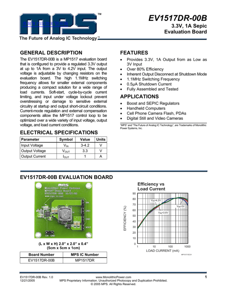
Over 80% Efficiency
Inherent Output Disconnect at Shutdown Mode
1.1MHz Switching Frequency
0.5µA Shutdown Current
Fully Assembled and Tested
•
•
•
•
•
APPLICATIONS
•
•
•
•
Boost and SEPIC Regulators
Handheld Computers
Cell Phone Camera Flash, PDAs
Digital Still and Video Cameras
“MPS” and “The Future of Analog IC Technology”, are Trademarks of Monolithic
Power Systems, Inc.
ELECTRICAL SPECIFICATIONS
Parameter
Input Voltage
Output Voltage
Output Current
Symbol
Value
Units
VIN
VOUT
IOUT
3-4.2
3.3
1
V
V
A
EV1517DR-00B EVALUATION BOARD
Efficiency vs
Load Current
90
EFFICIENCY (%)
80
VIN=4.2V
70
VIN=3V
60
VIN=3.6V
50
40
30
20
10
(L x W x H) 2.0” x 2.0” x 0.4”
(5cm x 5cm x 1cm)
Board Number
MPS IC Number
EV1517DR-00B
MP1517DR
EV1517DR-00B Rev. 1.0
12/21/2005
0
1
10
100
1000
LOAD CURRENT (mA)
www.MonolithicPower.com
MPS Proprietary Information. Unauthorized Photocopy and Duplication Prohibited.
© 2005 MPS. All Rights Reserved.
MP1517-EC01
1
TM
EV1517DR-00B – 3.3V, 1A SEPIC EVALUATION BOARD
查询"MP1517DR"供应商
EVALUATION BOARD SCHEMATIC
VIN
3V - 4.2V
GND
U1
4
EN
D2
1N4148
8
IN
SW
EN
GND
SW
15
SS
C4
10nF
MP1517
3
FB
BP
C5
10nF
COMP
7
OLS
SGND SGND
5
13
VOUT
10
3.3V/1A
D1
B340A-13
3A
9
GND
16
1
PGND PGND
11
T1
DRQ125-3R3
12
C3
4.7nF
C6
NS
EV1517_S01
EV1517DR-00B BILL OF MATERIALS
Qty
Ref
Value Description
Package Manufacturer Manufacturer P/N
2
C1A, C1B
10µF
Ceramic Cap, 6.3V, X5R
1210
TDK
2
C2A, C2B
22µF
Ceramic Cap, 6.3V, X7R
1210
TDK
1
C3
0805
Panasonic
2
C4, C5
4.7nF Ceramic Cap, 50V, X7R
10nF Ceramic Cap, 50V, X7R
0805
TDK
C3225X5R1A106K
C3225X5R0J226M
ECJ-2VB1H472K
C2012X7R1H103K
1
C6
1
C7
Ceramic Cap, 10V, X5R
0805
TDK
C2012X5R1A105K
1
C8
4.7uF Ceramic Cap, 10V, X5R
0805
Panasonic
ECJ-2FB1A475K
1
D1
Diodes Inc
B340LA-13-F
1
D2
1
R1
1
R2
1
R3
1
R4
5.1KΩ Film Resistor, 5%
100KΩ Film Resistor, 5%
1
T1
3.3uH Coupled Inductors, 4.63A, SMD
1
U1
Do Not Stuff
1uF
Schottky Diode, 40V, 3A, SMA
Rectifier Diode, 75V, 200mW,
SOD-323
37.4KΩ Film Resistor, 1%
10KΩ Film Resistor, 1%
EV1517DR-00B Rev. 1.0
12/21/2005
DC-DC Converter
Diodes Inc
1N4148WS-7
0805
Panasonic
ERJ-6ENF3742V
0805
Panasonic
ERJ-6ENF1002V
0805
Panasonic
ERJ-6GEYJ512V
0805
Panasonic
ERJ-6GEYJ104V
Cooper
DRQ125-3R3
MPS
MP1517DR
www.MonolithicPower.com
MPS Proprietary Information. Unauthorized Photocopy and Duplication Prohibited.
© 2005 MPS. All Rights Reserved.
2
TM
EV1517DR-00B – 3.3V, 1A SEPIC EVALUATION BOARD
查询"MP1517DR"供应商
PRINTED CIRCUIT BOARD LAYOUT
Figure 1—Top Silk Layer
Figure 2—Top Layer
Figure 3—Bottom Layer
EV1517DR-00B Rev. 1.0
12/21/2005
www.MonolithicPower.com
MPS Proprietary Information. Unauthorized Photocopy and Duplication Prohibited.
© 2005 MPS. All Rights Reserved.
3
TM
EV1517DR-00B – 3.3V, 1A SEPIC EVALUATION BOARD
查询"MP1517DR"供应商
QUICK START GUIDE
The output voltage of this board is set to 12V. The board layout accommodates most commonly used
inductors and output capacitors.
1. Preset Power Supply to 3V ≤ VIN ≤ 4.2V.
2. Turn Power Supply off.
3. Connect Power Supply terminals to:
Positive (+): VIN, EN
Negative (–): GND
4. Connect Load to:
Positive (+): VOUT
Negative (–): GND
5. Turn Power Supply on after making connections.
6. The MP1517 is enabled on the evaluation board once VIN is applied. To disable the MP1517,
disconnect EN from VIN.
7. The output voltage VOUT can be changed by varying R1. Calculate the new value using the
formula:
⎛V
⎞
R1 = ⎜⎜ OUT − 1⎟⎟R2
⎝ VFB
⎠
Where VFB = 0.7V and R2 = 10kΩ
For example, for VOUT = 3.6V
⎛ 3 .6 V
⎞
− 1⎟ × 10kΩ = 41.4kΩ
R1 = ⎜
⎝ 0 .7 V
⎠
Therefore use a 41.2kΩ standard 1% value resistor.
NOTICE: The information in this document is subject to change without notice. Please contact MPS for current specifications.
Users should warrant and guarantee that third party Intellectual Property rights are not infringed upon when integrating MPS
products into any application. MPS will not assume any legal responsibility for any said applications.
EV1517DR-00B Rev. 1.0
12/21/2005
www.MonolithicPower.com
MPS Proprietary Information. Unauthorized Photocopy and Duplication Prohibited.
© 2005 MPS. All Rights Reserved.
4
