Product Not Recommended for New Designs
Application Note: Spartan-II and Spartan-3 Families, Virtex and Virtex-II Series
R
Analog Devices TigerSHARC Link
Author: Nick Sawyer
XAPP634 (v1.2) October 26, 2004
Summary
This application note describes a full-featured transmitter/receiver macro that can
communicate with Spartan™-II, Spartan-IIE, Spartan-3, Virtex™, Virtex-E, Virtex-II, and
Virtex-II Pro™ FPGA families via the Analog Devices ADSP-TS101S TigerSHARC™ link-port
function.
Introduction
The Analog Devices TigerSHARC Digital Signal Processors (DSPs) contain an optional linkport function that is intended for communication between DSPs, but can also be used to
communicate with Virtex series FPGAs. This is extremely useful when a system is designed
around these two components. The macro described herein is a full featured transmitter/
receiver compatible with ADSP-TS101S devices that allow bidirectional double data rate (DDR)
communication of 128-bit words over an 8-bit link at speeds of up to 125 megabits per second
(Mb/s) per line (125 megabytes per second (MB/s) total) in a Virtex-E -7 or a Spartan-3
-5 device and 167 Mb/s per line (167 MB/s total) in a Virtex-II -5 or a Virtex-II Pro -5 device. Full
details on the link port characteristics are available from Analog Devices at:
http://www.analog.com/processors/resources/technicalLibrary/manuals/index.html
Note: The macro described herein is intended for use in systems where the clock rate is the
same or very close (within 1,000 ppm) in the devices at each end of the link.
Circuit
Description
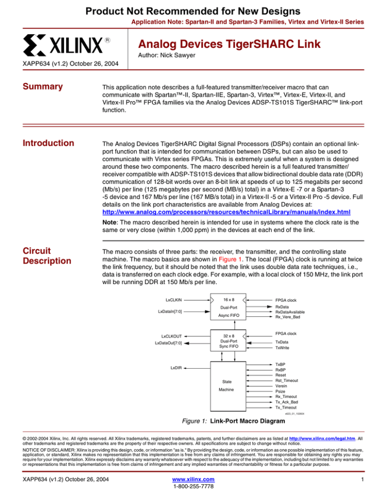
The macro consists of three parts: the receiver, the transmitter, and the controlling state
machine. The macro basics are shown in Figure 1. The local (FPGA) clock is running at twice
the link frequency, but it should be noted that the link uses double data rate techniques, i.e.,
data is transferred on each clock edge. For example, with a local clock of 150 MHz, the link port
will be running DDR at 150 Mb/s per line.
16 x 8
LxCLKIN
Dual-Port
LxDataIn[7:0]
Async FIFO
32 x 8
Dual-Port
Sync FIFO
LxCLKOUT
LxDataOut[7:0]
LxDIR
State
Machine
FPGA clock
RxData
RxDataAvailable
Rx_Vere_Bad
FPGA clock
TxData
TxWrite
TxBP
RxBP
Reset
Rst_Timeout
Verein
Psize
Rx_Timeout
Tx_Ack_Bad
Tx_Timeout
x623_01_102604
Figure 1: Link-Port Macro Diagram
© 2002-2004 Xilinx, Inc. All rights reserved. All Xilinx trademarks, registered trademarks, patents, and further disclaimers are as listed at http://www.xilinx.com/legal.htm. All
other trademarks and registered trademarks are the property of their respective owners. All specifications are subject to change without notice.
NOTICE OF DISCLAIMER: Xilinx is providing this design, code, or information "as is." By providing the design, code, or information as one possible implementation of this feature,
application, or standard, Xilinx makes no representation that this implementation is free from any claims of infringement. You are responsible for obtaining any rights you may
require for your implementation. Xilinx expressly disclaims any warranty whatsoever with respect to the adequacy of the implementation, including but not limited to any warranties
or representations that this implementation is free from claims of infringement and any implied warranties of merchantability or fitness for a particular purpose.
XAPP634 (v1.2) October 26, 2004
www.xilinx.com
1-800-255-7778
1
R
Product Not Recommended for New Designs
Analog Devices TigerSHARC Link
Receiver
When the macro is in receiver mode, the incoming data is clocked into a small dual-port FIFO.
Eight bits are clocked in by the rising edge of the incoming clock and eight bits by the falling
edge. This data is almost immediately clocked out of the FIFO synchronous to the FPGA clock
and is presented byte-wide to the user’s system with data valid timing. Data transfers are shown
in Figure 2, which shows the case where the VERE function (described below) is not used.
Figure 3 shows the case where the VERE function is enabled. The assumption here is that the
user logic will always be capable of accepting incoming data, or that a FIFO external to the
macro is available. Example designs of FIFOs that work with the link-port macro are given in
the reference design .zip file described in Design Files.
Single Transfer
FPGA Clock
RxData
b0
b1
b2
b14 b15
RxDataAvailable
Burst Transfer
FPGA Clock
RxData
b0
b1
b2
b14 b15
b0
b1
RxDataAvailable
x623_02_042502
Figure 2: Data Valid Timing (no VERE)
One characteristic of the link-port protocol is that it can be used with or without the transmission
of a verification byte. This VERE function is turned on or off via registers in the ADSP-TS101S
device, or by setting the signal “Verein” of the FPGA macro to 1. The VERE byte is not directly
available to the user, but when the function is enabled, the output Rx_Vere_Bad of the macro
indicates whether the last received 128-bit data was correctly received or not. The timing for
this signal is shown in Figure 3.
It is recommended to enable the VERE function for two reasons. The first is to ensure data
integrity, and the second is to minimize the possibility of data overrun, which could occur
between two systems that do not have exactly the same clock. The byte received immediately
following the VERE byte is undefined in the spec, and so is not useful as data, but very useful
for rate adaption. If the FPGA clock is running slower than the link clock, there will be only one
“blank” receive cycle during burst transfers every now and then. If the FPGA clock is running
synchronously to the DSP, the received word will always be followed by a VERE byte, followed
by a dummy byte. RxDataAvailable will be Low for both these bytes, as shown in Figure 3. If the
FPGA clock is running slightly faster than the DSP clock, the VERE byte will be followed by one
or two dummy bytes. If the FPGA clock is running slightly slower than the DSP clock, the VERE
byte will be followed either by a dummy byte or by the first byte of the next word in a burst
transfer. Thus, rate adaption is provided for in all three cases when the VERE function is
enabled, thus avoiding the overrun that could occur otherwise.
2
www.xilinx.com
1-800-255-7778
XAPP634 (v1.2) October 26, 2004
Product Not Recommended for New Designs
R
Analog Devices TigerSHARC Link
Single Transfer
FPGA Clock
b0
RxData
b1
b2
b14 b15 vere
RxDataAvailable
1 = bad
0 = good
Rx_Vere_Bad
Burst Transfer
FPGA Clock
RxData
b0
b1
b2
b14
B0 or
b15 vere XX
RxDataAvailable
1 = bad
0 = good
Rx_Vere_Bad
x623_03_042502
Figure 3: Data Valid Timing (with VERE)
Transmitter
Data (128-bit) for transmission is written to the macro using the timing shown in Figure 4.
FPGA Clock
TxData
b0
b1
b2
b3
b n b n+1 XX
XX bn+2 bn+3
TxWrite
TxBP
Stop Filling
Transmitter
Start Filling
Transmitter Again
x623_04_051402
Figure 4: Transmitter Timing
The input path is a shallow synchronous FIFO of 32 or 64 bytes that generates a back-pressure
signal (TxBP) when it is getting full. The user should not continue to write data when this backpressure signal is High or data will be lost. The user also needs to ensure that data is written in
multiples of 16 bytes, because there is no mechanism built into the macro to check for this and
it is otherwise possible that an underrun could occur. If the VERE data verification function has
been enabled, then the VERE byte is calculated by the macro and is automatically inserted into
the transmitted data as per the link-port specification. Note that the VERE function can only be
enabled or disabled for both the transmitter and the receiver. The parameter cannot be
individually used for the transmitter or the receiver.
XAPP634 (v1.2) October 26, 2004
www.xilinx.com
1-800-255-7778
3
R
Product Not Recommended for New Designs
Analog Devices TigerSHARC Link
State Machine
The state machine manages the receive and transmit functionality of the macro and provides
additional feedback signals to the user. Inputs to the state machine include the Verein input
described above that enables (High) or disables (Low) the VERE function. There is also a
“PSIZE” input that serves the same purpose as the PSIZE register bit in the ADSP-TS101S
device. When this is set Low, a maximum burst size of 64 transmissions is allowed, and when
set High, the burst size is set to infinity. There is an output signal called “Tx_Ack_Bad” that
indicates when the connectivity check specified by the link-port protocol has failed. This would
typically indicate a bad connection between systems.
Time-outs for both receiver and transmitter are also built in per the link-port specification. These
outputs will go High when a receive or transmit time-out has occurred. They are reset by setting
the "rst_timeout" input High for one clock cycle. If this input is unused, it should be connected
to a logic 0 for correct operation. These signals are not used internally to the macro.
Clocking
Considerations
The FPGA clock should be connected via a global buffer, but this is not so obvious for the
incoming link clock (LxCLKIN). This clock signal is fairly lightly loaded, with around ten clock
loads and six logic loads. The clock loads are used to clock in data, so ideally the clock would
be passed through a DLL/DCM to minimize the hold time at the pins. However, the signal is
non-continuous, and so this is not possible. If the clock is passed through a global buffer, then
the hold time at the inputs will be quite long at 1 ns to 2 ns, which is not a problem at low link
frequencies, but starts to become important over 100 Mb/s. The solution chosen is, therefore,
to use the clock signal directly and to apply a MAXSKEW or USELOWSKEWLINES constraint
to the net, to ensure that race conditions are avoided. This is applied to the design via a .ucf
constraint file, an example of which is given in the design .zip file in Design Files.
Top Level
The top level design to use the macro is shown in Figure 5. This basically combines the input
and output data busses into one bidirectional bus using 3-state buffers in the IOBs of the FPGA.
An example is given in the design .zip file. The output signals, i.e., LxData[7:0], LxDIR, and
LxClkout are driven by flip-flops in the IOBs of the FPGA to minimize skew between the clock
and the data signals. The control signal LxDIR is only used when using an external buffer for
level translation, which is typically not necessary. The transmission standard for the FPGA can
be any of the supported standards, but would typically be 3.3V LVTTL signaling as this is used
by the ADSP-TS101S. There are no constraints on where the link port pins should be located
on the device, other than they should be placed as close together as possible.
LxCLKIN
LxDATA[7:0]
Link
Port
Interface
LxCLOUT
LxCLKIN
LxDataIn[7:0]
LxCLOUT
Link
Port
Interface
LxDataOut[7:0]
LxDIR
LxDIR
x623_05_061102
Figure 5: Top-Level Design Diagram
4
www.xilinx.com
1-800-255-7778
XAPP634 (v1.2) October 26, 2004
Product Not Recommended for New Designs
Analog Devices TigerSHARC Link
R
Design Files
The macro design files are written for Virtex, Virtex-E, Virtex-II, and Virtex-II Pro devices. These
design files are available in both Verilog and VHDL from the Xilinx website (xapp634.zip). See
the readme.txt file enclosed in the zip file for the latest details.
Conclusion
Spartan and Virtex series devices can be easily interfaced with Analog Devices ADSP-TS101S
devices, using the macro described in this application note for the embedded link port function,
at link speeds of up to 150 Mb/s. This allows the rapid and transparent transfer of data between
the DSP and the FPGA in applications where, for instance, an algorithm is shared between
software and hardware.
Revision
History
The following table shows the revision history for this document.
Date
Version
06/21/02
1.0
Initial Xilinx release.
03/17/04
1.1
Deleted text from Transmitter section. Updated Web links. Added
Spartan-3 devices to mentioned Xilinx FPGA families.
10/26/04
1.2
Revised Figure 1.
XAPP634 (v1.2) October 26, 2004
Revision
www.xilinx.com
1-800-255-7778
5


