International Journal of Science, Engineering and Technology Research (IJSETR), Volume 4, Issue 4, April 2015
A Novel control topology of Quasi ZSI based
PV systems
Mr.Javid Ahamed.S1, Mr.Mahendiran.C.R2., Mr.Ram Kumar.M3
Abstract— This paper shows the clear understanding of the
control of the output voltage by varying the modulation index
and the boost factor independently. A comparative analysis
between impedance source inverter and the quasi impedance
source inverter(QZSI) were made and the best suitable inverter
for PV generation system is found. The closed loop strategy in
the QZSI were implemented successfully with good power
conversion. The unique gate pulse pattern is designed to cope up
with the shoot through and non-shoot through states in
MATLAB Simulink and the gate pulse pattern is generated
using the PIC 16F877A..
Index Terms—Boost factor, MATLAB Simulink, Modulation
Index, PV systems, Quasi Impedance Source Inverter,
1)INTRODUCTION
The Alternative resources are in great demand nowadays.
The traditional resources are reducing across the world
rapidly. One of the popular alternative resources is the
generation of electrical power from the PV panel. Many
research efforts are made to extract maximum power out of
the PV panel by using different power converters as most of
the power generated by the renewable sources are varying.
There are different traditional power circuit topologies which
has many disadvantages. The conventional Voltage Source
Inverters(VSI) and DC/DC converters have certain
disadvantages such as double stage conversion, maximum
output voltage obtained is less than the dc voltage, complexity
in the controller circuits and the inverter components should
be oversized to match with the continuous variation of PV
voltages which can be overcome by the proposed control
topology of quasi impedance source inverter. This paper
mainly focuses on the simulation of the open loop and closed
loop implementation of the quasi impedance source inverter
connected to the PV systems in which the output voltage can
be controlled by both modulation index and the boost factor
independently. This advantage makes PV generation more
efficient. As the quasi impedance source inverter has the
advantage of having no dead time. It is designed to operate in
one of the mode named shoot through mode whether the same
leg switches(upper leg and lower leg) are short switched ON
so that short circuit occurs whereas in traditional VSI methods
we are forced to make the dead time in order to avoid the short
circuit of the same leg. A comparative analysis between
impedance source and the quasi impedance source inverter
were done to find out the best topology for the PV systems.
.
2)QZI SOURCE TOPOLOGY
The Quasi Impedance source network is introduced after the
introduction of the Impedance source inverter. This Quasi
Impedance source inverter overcomes certain disadvantages
of the Impedance source inverter. The quasi Impedance
Source inverter has advantages over impedance source
inverter such as continuous input current, higher reliability,
causes less EMI problems, reduced source stress, reduced
component ratings and simple control strategy. This is the
most adaptive topology of PV generation systems to offer
good conversion efficiency. The Quasi Impedance source
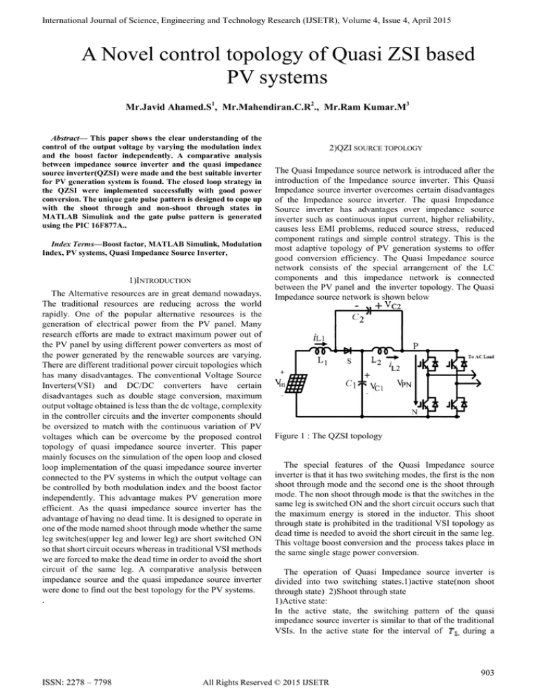
network consists of the special arrangement of the LC
components and this impedance network is connected
between the PV panel and the inverter topology. The Quasi
Impedance source network is shown below
Figure 1 : The QZSI topology
The special features of the Quasi Impedance source
inverter is that it has two switching modes, the first is the non
shoot through mode and the second one is the shoot through
mode. The non shoot through mode is that the switches in the
same leg is switched ON and the short circuit occurs such that
the maximum energy is stored in the inductor. This shoot
through state is prohibited in the traditional VSI topology as
dead time is needed to avoid the short circuit in the same leg.
This voltage boost conversion and the process takes place in
the same single stage power conversion.
The operation of Quasi Impedance source inverter is
divided into two switching states.1)active state(non shoot
through state) 2)Shoot through state
1)Active state:
In the active state, the switching pattern of the quasi
impedance source inverter is similar to that of the traditional
VSIs. In the active state for the interval of
during a
903
ISSN: 2278 – 7798
All Rights Reserved © 2015 IJSETR
International Journal of Science, Engineering and Technology Research (IJSETR), Volume 4, Issue 4, April 2015
switching cycle of time period T. The voltage equations are
given below,
(3)
From the above equations (2) and (3),
(1)
(4)
In the steady state, the average value of the inductor
over
one switching period of T will be zero from (1) and (2),
(5)
Figure 2: Equivalent circuit of Active state
And from equations (3),(5) and (6)
2)Shoot through mode:
In this mode the switches in the same leg are switched on
for a very short period of time. The input voltage will not get
short circuited but instead the voltage gets boosted due to the
presence of LC network. In the active state for the interval of
during a switching cycle of time period T. The voltage
equations are given as follows,
The dc link voltage we obtained is the sum of the capacitor
voltages
and
,
(6)
(7)
The dc link voltage will be the multiplication of the boost
factor and the input voltage. So, the output voltage will be the
product of the boost factor B and the modulation index M.
Thus in our proposed control topology of the PV panel the
boost factor and the modulation index are changed separately
to control the inverted output voltage.
(2)
3)SIMULATION RESULTS
Figure 2: Equivalent circuit of Shoot through state
In the steady state, the average value of the inductor
over
one switching period of T will be zero from (1) and (2),
The special gate pulse generation for the quasi
impedance source inverter were done using the MATLAB
Simulink. In the proposed gate pulse specific pattern which
makes the output voltage very effective and the power
conversion efficiency was better than the other methods.
For this different kind of gate signals for the switches(S1 to
S4) two PWM strategies were used. One for constant PWM
and the other for the sinusoidal PWM. The sinusoidal PWM is
done by comparing the sinusoidal voltage of 50Hz with the
triangular wave of frequency 3kHz.The constant PWM can be
done by varying the constant voltage with the triangular wave
of the same frequency. The comparison of sinusoidal wave
and the triangular wave is given below.
904
ISSN: 2278 – 7798
All Rights Reserved © 2015 IJSETR
International Journal of Science, Engineering and Technology Research (IJSETR), Volume 4, Issue 4, April 2015
Figure 4:Comparison of triangular wave and the sinusoidal
wave
Figure 6: Gate signals obtained which is to be given to all the
four switches
The output frequency is made as 50Hz.So,the duration of
ON and OFF time of the lower leg switches are made
according to 50Hz.The gate pulse pattern are generated such
that during the first half of the full time period T one of the
lower leg switch(S2) is ON and the other lower leg switch(S4)
is OFF. During this first half of the total time period T the
upper leg switch(S1) is switched under the sinusoidal PWM
and another upper leg switch(S3) is switched under constant
PWM. During the next half of the time period the gate pulse
pattern reverses. This kind of gate pulse pattern have
independent control of the output voltage by varying the
modulation index and the boost factor. This proposed gate
pulse pattern provides good results during the shoot through
and the non-shoot through modes of the quasi impedance
source inverter.
The following figure shows the special pattern of
generating the gate pulse done in the MATLAB Simulink.
The above mentioned type of gate pulse pattern is generated
using the help of the MATLAB Simulink blocks in the library
Assume a PV panel which offers 24V continuously in
which it is connected to impedance network and the output
voltage is simulated. This whole topology is done in the
MATLAB Simulink.
Figure 7:MATLAB Simulink model for the Quasi
Impedance Source inverter
Figure 5:MATLAB Simulink Model for Gate pulse
generation
The following figure shows the gate pulse pattern for the
quasi impedance source inverter in the MATLAB simulink.
The pattern is generated for all the switches present in the
quasi impedance source inverter as shown below.
topology for the PV generation.
In the open loop condition the whole circuit is investigated
in two cases. In the first case the modulation index is kept
constant and the boost factor is varied and in the other case the
modulation index is varied and the boost factor is kept
constant. The output voltage for the modeled Quasi
Impedance source inverter was taken from the MATLAB
simulink workspace. The simulation was done for different
values of modulation index and boost factor for both
impedance source and quasi impedance source inverter and
the results were tabulated to find out the best inverter
The parameters used in the system are tabulated as follows
905
ISSN: 2278 – 7798
All Rights Reserved © 2015 IJSETR
International Journal of Science, Engineering and Technology Research (IJSETR), Volume 4, Issue 4, April 2015
Input Voltage Vin(app)
24V
Output frequency
50Hz
Switching frequency
3kHz
Capacitance C1,C2
1000e-6micro Farad
Inductance L1,L2
1e-6
Power rating
240W
Table 1 : Parameters used in the simulation of the topology
PV generation system.
The prolific waveform which is obtained for different cases
of the modulation index and the boost factor is shown as
below.
By varying the boost factor as 0.5,0.6,0.7,0.8 and keeping
the modulation index 0.5 as constant for the solar input
voltage of Vin=24V.
The output voltages of the impedance source inverter and the
quasi impedance source inverter were taken by keeping the
modulation index MI=0.923 and by varying the boost factor.
Boost Factor
Impedance source
inverter(Vout)
0.9
74.2
Quasi Impedance
source
inverter(Vout)
329.5
0.8
97.3
368.5
0.7
99.8
393.3
0.6
101.6
408.6
0.5
102.8
421.2
0.4
107.4
431.23
0.3
113.3
438.5
0.2
170.6
444.3
0.1
300
380.3
Table 2 : Comparison of the output voltage between
impedance and trans impedance inverters with Rload
Vin=24V,MI=0.923 by varying the Vmpp.
The output voltages of the respective inverter by keeping
MI=0.5 and by varying the boost factor is tabulated as
follows.
Boost Factor
Impedance source
inverter(Vout)
0.9
77.5
Quasi Impedance
source
inverter(Vout)
330.1
0.8
102.5
369.1
0.7
101.74
392.2
0.6
102.74
409.7
0.5
103.8
421.5
0.4
107.8
431.5
0.3
113.2
438.5
0.2
170.2
444.42
0.1
102.5
380.18
Figure 8: R load with MI=0.5 and Vmpp=0.5,0.6,0.7,0.8,.9
for Vin=24V respectively for trans impedance source inverter
By varying the modulation index as 0.3,0.5,0.8 and 0.9 and
keeping the boost factor 0.4 as constant for the solar input
voltage of Vin=24V the following waveforms were obtained.
Table 3 : Comparison of the output voltage between
impedance and trans impedance inverters with Rload
Vin=24V,MI=0.5 by varying the Vmpp.
By the above mentioned collected data we conclude that
the quasi impedance source inverter is the better option for the
906
ISSN: 2278 – 7798
All Rights Reserved © 2015 IJSETR
International Journal of Science, Engineering and Technology Research (IJSETR), Volume 4, Issue 4, April 2015
The output voltage which is obtained from this closed loop
operation of the Quasi Impedance source produces the
capacitor voltage and the peak value of the capacitor voltage
is compared with the reference voltage which is then given to
the PI controller. Then the output of the PI controller is given
to the boost factor which is then compared with the triangular
wave to produce the pulse. This is the appropriate method of
controlling the Quasi Impedance source inverter with the PV
generation systems
Figure 11: The output voltage of the closed loop operation of
the Quasi Impedance source inverter
Figure 9: R load with MI=0.3,0.5,0.8,0.9 and Vmpp=0.4 for
Vin=24V trans impedance source inverter
In the closed loop condition the capacitor voltage is taken
and is compared with the reference voltage which is then
given to the boost factor to produce the maximum output
voltage.
Figure 12: The capacitor voltage(C1) of the closed loop
operation
A comparative analysis is made between impedance source
inverter and quasi impedance source inverter and it is
concluded that quasi impedance source inverter with this
specific gate pulse pattern and the control circuit is found to
be most suitable than any other traditional inverters.
4)GATE PULSE PATTERN GENERATED
THROUGH PIC 16F877A
Figure 10:Closed loop topology of the QZSI
The PIC16F877A microprocessor manufactured by Texas
instruments is a high performance, highly integrated
processor used as a controller for the inverter circuit. The
PIC16F877A has a C Compiler Optimized Architecture with
Optional Extended Instruction Set. It consists of 100,000
Erase/Write Cycle Enhanced Flash and its program memory
is typical one. Flexible oscillator option is available in this
PIC16F877A. It includes Four Crystal modes, including
High-Precision PLL for USB. It has two External Clock
modes, Up to 48 MHz. The Internal Oscillator consists of 8
user-selectable frequencies, from 31 kHz to 8 MHz Dual
907
ISSN: 2278 – 7798
All Rights Reserved © 2015 IJSETR
International Journal of Science, Engineering and Technology Research (IJSETR), Volume 4, Issue 4, April 2015
Oscillator Options allow Microcontroller and USB module to
run at different Clock Speeds. These features makes the PIC
microcontroller PIC16F877A most suitable for generating the
specified pulses.
The proposed gate signal is programmed and generated
using the PIC microcontroller 16F877A which can be used to
drive the power electronic switches through the gate driver IC
which is suitable.
Figure 13 : Gate pulse pattern for all the switches which are
generated using the PIC 1F877A
5)CONCLUSION
In this paper, the interface between the PV dc source and
the load is accomplished by a Quasi Impedance source
inverter. The unique gate pulse pattern is simulated in
MATLAB for the impedance source network and trans
impedance source network. Both impedance source inverter
and the trans impedance source inverters are simulated in
MATLAB simulink and the output voltages are compared and
tabulated by changing various values of the maximum voltage
and keeping modulation index as constant and vice versa. The
trans impedance source inverter was found to be more
advantageous than others due to the advantages of single stage
power conversion, increased voltage gain and reduced
voltage stress. The gate pulse pattern is coded and
implemented in the real time implementation.
TRANSACTIONS ON SUSTAINABLE ENERGY, VOL. 4,
NO. 1, JANUARY 2013.
[2]Y. Li, J. Anderson, F. Z. Peng, and D. Liu,
“Quasi-Z-source inverter for photovoltaic systems,” in
Proc. IEEE APEC, 2009, pp. 918–924.
[3]Yuan Li,Joel Anderson,Fang Z. Peng and Dichen Liu”
Quasi-Z-Source Inverter for Photovoltaic Power
Generation Systems”,IEEE 2009.
[4]M. Shahparasti, Student Member, A. Sadeghi
Larijani, Student Member, IEEE, A. Fatemi, Yazdian
Varjani, Member, IEEE and M. Mohammadian ,
Member, IEEE, Quasi Z-source Inverter for Photovoltaic
System Connected to Single Phase AC Grid” 1st Power
Electronic & Drive Systems & Technologies Conference.
[5] T.W. Chun1, H.H.Lee1, H.G.Kim2 and E.C.Nho3
Power Control for a PV Generation System
Using a Single-Phase Grid-Connected Quasi ZSource
Inverter 8th International Conference on Power Electronics ECCE Asia May 30-June 3, 2011, The Shilla Jeju, Korea.
[6] J. H. Park, H. G. kim, E. C. Nho, T. W. Chun and J
Choi. “Gridconnected PV System Using a Quasi-Z-source
Inverter,” in Proc. 2009
IEEE Applied Power Electronics Conf., pp. 925-929.
[7] F. Z. Peng, “Z-Source Inverter,” IEEE Trans. on Ind.
Appl., vol. 39, no.2, pp. 504-510, March/April. 2003.
JAVID AHAMED.S Author received B.E degree
in Electrical & Electronics in PSNA college of Engineering
and technology dindigal. He is pursuing Master of
Technology in Power electronics and drives at B.S.Abdur
Rahman University Vandalur Chennai.
MAHENDIRAN C R. Author received B.E
degree in Electrical &
Electronics in Sri Sairam
Engineering College Chennai. He is pursuing Master of
Engineering in Power system engineering at B.S.Abdur
Rahman University Vandalur Chennai.
RAM KUMAR M. is working as an Assistant
professor in the Department of Electrical & Electronics at
B.S. Adbur Rahman University. His area of interest is in
Converters, Embedded systems ,Solar energy and Fuel cells.
He also has a experience in the field of Electrical
Maintanance. He attended and many National level confere
REFERENCES
[1]Z. Peng,Yuan Li and Ge Baoming,”Quasi-Z-Source
Inverter-Based Photovoltaic Generation System With
Maximum Power Tracking Control Using ANFIS” IEEE
908
ISSN: 2278 – 7798
All Rights Reserved © 2015 IJSETR


