IRF630 - Taitron
advertisement
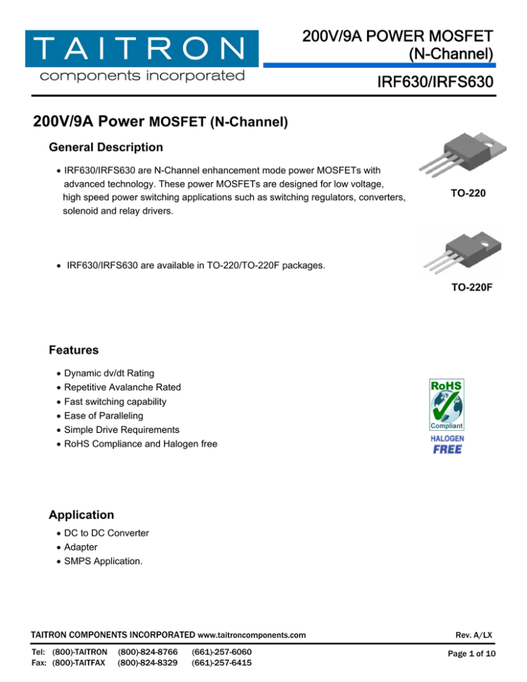
200V/9A POWER MOSFET (N-Channel) IRF630/IRFS630 200V/9A Power MOSFET (N-Channel) General Description • IRF630/IRFS630 are N-Channel enhancement mode power MOSFETs with advanced technology. These power MOSFETs are designed for low voltage, high speed power switching applications such as switching regulators, converters, solenoid and relay drivers. TO-220 • IRF630/IRFS630 are available in TO-220/TO-220F packages. TO-220F Features • • • • • • Dynamic dv/dt Rating Repetitive Avalanche Rated Fast switching capability Ease of Paralleling Simple Drive Requirements RoHS Compliance and Halogen free Application • DC to DC Converter • Adapter • SMPS Application. TAITRON COMPONENTS INCORPORATED www.taitroncomponents.com Tel: (800)-TAITRON Fax: (800)-TAITFAX (800)-824-8766 (800)-824-8329 (661)-257-6060 (661)-257-6415 Rev. A/LX Page 1 of 10 200V/9A POWER MOSFET (N-Channel) IRF630/IRFS630 Ordering Information Outline Part Number Packing Type/Qty’s TO-220 IRF630 Tube/50pcs TO-220F IRFS630 Tube/50pcs Pin Configuration and Symbol 1: GATE 2: DRAIN 3: SOURCE 1: GATE 2: DRAIN 3: SOURCE TO-220 TO-220F Absolute Maximum Ratings (TC=25ºC unless otherwise specified, Note) Symbol Description Ratings Unit VDSS Drain-Source Voltage 200 V VGSS Gate-Source Voltage ± 30 V Drain Current -Continuous 9 A Drain Current -Pulsed (Note1) 36 A ID IDM EAS EAR IAR dv/dt Avalanche Energy Single Pulsed (Note2) 250 Repetitive (Note1) 7.4 mJ Avalanche Current (Note1) 9 A Peak Diode Recovery dv/dt (Note3) 5 V/ns Rev. A/LX www.taitroncomponents.com Page 2 of 10 200V/9A POWER MOSFET (N-Channel) IRF630/IRFS630 Symbol Description Power Dissipation PD Derate above 25°C RθJA Thermal Resistance (Junction-to-Ambient) RθJC Thermal Resistance (Junction-to-Case) TJ Ratings TO-220 74 TO-220F 38 TO-220 0.58 TO-220F 0.3 TO-220/TO-220F 62 TO-220 1.71 TO-220F 3.3 Unit W W/°C °C/ W °C/ W Operating Junction Temperature -55 to +150 °C TSTG Storage Temperature Range -55 to +150 °C TL Maximum Lead Temperature for soldering purposes,1/8” from case for 10 seconds 300 °C Note: Absolute maximum ratings indicate limits beyond which damage to the device may occur. For guarantee specifications and test conditions, see the Electrical Characteristics. The guaranteed specifications apply only for the test conditions listed. Electrical Characteristics (TC=25ºC unless otherwise specified) Symbol Description Min. Typ. Max. Unit Conditions 200 - - V VGS=0V, ID=250µA - - 1 OFF CHARACTERISTICS V(BR)DSS Drain-Source Breakdown Voltage IDSS Drain-Source Leakage Current IGSS Gate-Source Leakage Current μA VDS=200V, VGS=0V VDS=160V, VGS=0V, TJ=125° C VGS=30V, VDS=0V - - 50 Forward - - 100 Reverse - - -100 2.0 - 4.0 V VDS=VGS, ID=250uA - - 0.4 Ω VGS=10V, ID=5.4A 3.8 - - S VDS=50V, ID=5.4A pF VDS=25V, VGS=0V, f=1.0MHz nA VGS=-30V, VDS=0V ON CHARACTERISTICS VGS(th) RDS(ON) gFS Gate-Source Threshold Voltage Static Drain-Source On-State Resistance (Note 4) Forward Transconductance DYNAMIC CHARACTERISTICS Ciss Input Capacitance - 800 - Coss Output Capacitance - 240 - Crss Reverse Transfer Capacitance - 76 Rev. A/LX www.taitroncomponents.com Page 3 of 10 200V/9A POWER MOSFET (N-Channel) IRF630/IRFS630 Symbol Description Min. Typ. Max. Unit Conditions nS VDD =100V, ID=5.9A, RG=12Ω, RD=16Ω (Note 4) nC VDS =160V, ID=5.9A, VGS =10V (Note 4) nH measured from the drain lead 0.25” from package to center of die measured from the drain lead 0.25” from package to source bond pad VGS =0V, Is=9A (Note 4) SWITCHING CHARACTERISTICS td(on) Turn-on Delay Time - 9.4 - tr Turn-on Rise Time - 28 - td(off) Turn-off Delay Time - 39 - tf Turn-off Fall Time - 20 - Qg Total Gate Charge - - 43 Qgs Gate-Source Charge - - 7 Qgd Gate-Drain Charge - - 23 Internal Drain inductance - 4.5 - Ld Ls Internal Drain inductance - 7.5 - DRAIN-SOURCE DIODE CHARACTERISTICS AND MAXIMUM RATINGS VSD Drain-Source Diode Forward Voltage - - 2 V trr Reverse Recovery Time - 170 340 nS Qrr Reverse Recovery Charge - 1.1 2.2 uC ton Forward turn-on time (Note5) - * - - Note VGS =0V, IF=5.9A di/dt=100A/us (Note4) 1: Repetitive Rating: Pulse width limited by maximum junction temperature 2: L=4.6mH, IAS=9A, VDD=50V, RG=25Ω, Starting TJ=25°C 3: Isd≤9A, di/dt≤120A/us, VDD≤VBR(DSS), Starting TJ=25°C 4: Pulse test: Pulse width ≤300us, Duty cycle≤2% 5: *Negligible, Dominated by circuit inductance Rev. A/LX www.taitroncomponents.com Page 4 of 10 200V/9A POWER MOSFET (N-Channel) IRF630/IRFS630 Typical Characteristics Curves Fig.2- Transconductance Variation Vs.Drain Current and Temperature Drain Current ID (A) Transconductance gFS (S) Fig.1- On-Region Characteristics Drain Current ID (A) Fig.3- Drain Current Variation Vs. Gate Voltage and Temperature Fig.4- Body Diode Forward Voltage Variation Vs. Current and Temperature Drain Current ID (A) Reverse Drain Current IDR (A) Drain-Source Voltage VDS (V) Gate-Source Voltage VGS (V) Body Diode Forward Voltage VSD (V) Rev. A/LX www.taitroncomponents.com Page 5 of 10 200V/9A POWER MOSFET (N-Channel) IRF630/IRFS630 Fig.6- On Resistance Variation Vs. Temperature Drain-Source On-Resistance RDS(ON) (Normalized) Drain-Source Breakdown Voltage V(BR)DSS (Normalized) Fig.5- Breakdown Voltage Variation Vs. Temperature Junction Temperature TJ (°C) Junction Temperature TJ (°C) Capacitance (pF) Fig.7- Capacitance Characteristics Drain-Source Voltage VDS (V) Rev. A/LX www.taitroncomponents.com Page 6 of 10 200V/9A POWER MOSFET (N-Channel) IRF630/IRFS630 Fig.8- Max. Safe Operation Area (TO-220) Drain Current ID (A) Drain Current ID (A) Fig.9- Max. Safe Operation Area (TO-220F) Fig.10- Transient Thermal Response (TO-220) Time (mS) Drain-Source Voltage VDS (V) Normalized Effective Transient Thermal Resistance r(t) Normalized Effective Transient Thermal Resistance r(t) Drain-Source Voltage VDS (V) Fig.11- Transient Thermal Response (TO-220F) Time (mS) Rev. A/LX www.taitroncomponents.com Page 7 of 10 200V/9A POWER MOSFET (N-Channel) IRF630/IRFS630 Dimensions in mm (Inch) TO-220 Rev. A/LX www.taitroncomponents.com Page 8 of 10 200V/9A POWER MOSFET (N-Channel) IRF630/IRFS630 TO-220F Rev. A/LX www.taitroncomponents.com Page 9 of 10 200V/9A POWER MOSFET (N-Channel) IRF630/IRFS630 How to contact us: US HEADQUARTERS 28040 WEST HARRISON PARKWAY, VALENCIA, CA 91355-4162 Tel: (800) TAITRON (800) 824-8766 (661) 257-6060 Fax: (800) TAITFAX (800) 824-8329 (661) 257-6415 Email: taitron@taitroncomponents.com Http://www.taitroncomponents.com TAITRON COMPONENTS MEXICO, S.A .DE C.V. BOULEVARD CENTRAL 5000 INTERIOR 5 PARQUE INDUSTRIAL ATITALAQUIA, HIDALGO C.P. 42970 MEXICO Tel: +52-55-5560-1519 Fax: +52-55-5560-2190 TAITRON COMPONENTS INCORPORATED REPRESENTAÇÕES DO BRASIL LTDA RUA DOMINGOS DE MORAIS, 2777, 2.ANDAR, SALA 24 SAÚDE - SÃO PAULO-SP 04035-001 BRAZIL Tel: +55-11-5574-7949 Fax: +55-11-5572-0052 TAITRON COMPONENTS INCORPORATED, SHANGHAI REPRESENTATIVE OFFICE METROBANK PLAZA, 1160 WEST YAN’ AN ROAD, SUITE 1503, SHANGHAI, 200052, CHINA Tel: +86-21-5424-9942 Fax: +86-21-5424-9931 Rev. A/LX www.taitroncomponents.com Page 10 of 10
