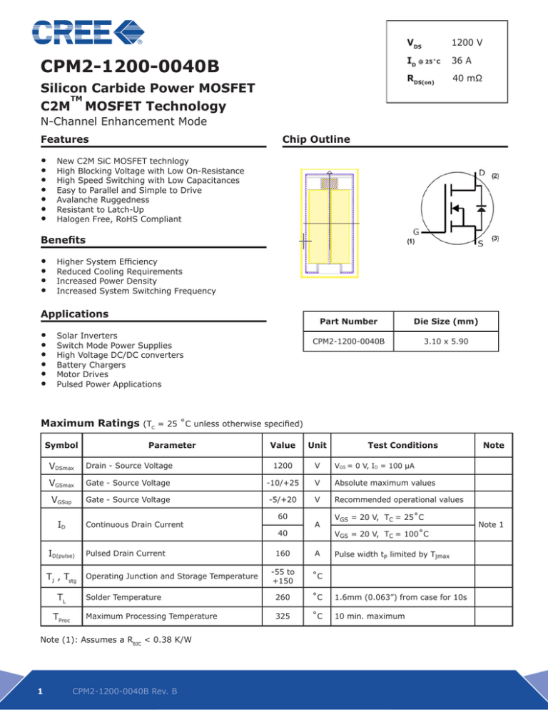
VDS
1200 V
ID @ 25˚C 36 A
CPM2-1200-0040B
Silicon Carbide Power MOSFET
TM
C2M MOSFET Technology
RDS(on)
40 mΩ
N-Channel Enhancement Mode
Features
•
•
•
•
•
•
•
Chip Outline
New C2M SiC MOSFET technlogy
High Blocking Voltage with Low On-Resistance
High Speed Switching with Low Capacitances
Easy to Parallel and Simple to Drive
Avalanche Ruggedness
Resistant to Latch-Up
Halogen Free, RoHS Compliant
Benefits
•
•
•
•
Higher System Efficiency
Reduced Cooling Requirements
Increased Power Density
Increased System Switching Frequency
Applications
•
•
•
•
•
•
Solar Inverters
Switch Mode Power Supplies
High Voltage DC/DC converters
Battery Chargers
Motor Drives
Pulsed Power Applications
Part Number
Die Size (mm)
CPM2-1200-0040B
3.10 x 5.90
Maximum Ratings (TC = 25 ˚C unless otherwise specified)
Symbol
Parameter
Unit
Test Conditions
VDSmax
Drain - Source Voltage
1200
V
VGS = 0 V, ID = 100 μA
VGSmax
Gate - Source Voltage
-10/+25
V
Absolute maximum values
VGSop
Gate - Source Voltage
-5/+20
V
Recommended operational values
ID
Continuous Drain Current
ID(pulse)
Pulsed Drain Current
TJ , Tstg
Operating Junction and Storage Temperature
TL
TProc
60
40
A
VGS = 20 V, TC = 25˚C
VGS = 20 V, TC = 100˚C
160
A
-55 to
+150
˚C
Solder Temperature
260
˚C
1.6mm (0.063”) from case for 10s
Maximum Processing Temperature
325
˚C
10 min. maximum
Note (1): Assumes a RθJC < 0.38 K/W
1
Value
CPM2-1200-0040B Rev. B
Pulse width tP limited by Tjmax
Note
Note 1
Electrical Characteristics (TC = 25˚C unless otherwise specified)
Symbol
Parameter
V(BR)DSS
Drain-Source Breakdown Voltage
VGS(th)
Gate Threshold Voltage
IDSS
Zero Gate Voltage Drain Current
IGSS
Gate-Source Leakage Current
RDS(on)
Min.
Typ.
Max. Unit
1200
V
VGS = 0 V, ID = 100 μA
2.4
2.8
V
VDS = 10 V, ID = 10mA
1.8
2.0
V
VDS = 10 V, ID = 10mA,TJ = 150 °C
100
μA
VDS = 1200 V, VGS = 0 V
250
nA
VGS = 20 V, VDS = 0 V
1
40
Drain-Source On-State Resistance
52
84
15.1
Transconductance
Ciss
Input Capacitance
Coss
Output Capacitance
Crss
Reverse Transfer Capacitance
10
Eoss
Coss Stored Energy
82
μJ
EAS
Avalanche Energy, Single Pluse
2
J
EON
Turn-On Switching Energy
1.0
EOFF
Turn Off Switching Energy
0.4
td(on)
Turn-On Delay Time
15
Rise Time
52
Turn-Off Delay Time
26
Fall Time
34
Internal Gate Resistance
1.8
Qgs
Gate to Source Charge
28
Qgd
Gate to Drain Charge
37
Qg
Total Gate Charge
td(off)
tf
RG(int)
VGS = 20 V, ID = 40 A
mΩ
gfs
tr
Test Conditions
VGS = 20 V, ID = 40 A, TJ = 150 °C
VDS= 20 V, IDS= 40 A
S
13.2
VDS= 20 V, IDS= 40 A, TJ = 150 °C
1893
VGS = 0 V
150
pF
VDS = 1000 V
Note
Fig. 11
Fig.
4,5,6
Fig. 7
Fig.
17,18
f = 1 MHz
VAC = 25 mV
Fig 16
ID = 40A, VDD = 50V
Fig. 29
mJ
VDS = 800 V, VGS = -5/20 V
ID = 40A, RG(ext) = 2.5Ω, L= 80 μH
Fig. 25
ns
VDD = 800 V, VGS = -5/20 V
ID = 40 A
RG(ext) = 2.5 Ω, RL = 20 Ω
Timing relative to VDS
Per IEC60747-8-4 pg 83
Fig. 27
Ω
f = 1 MHz, VAC = 25 mV
nC
VDS = 800 V, VGS = -5/20 V
ID = 40 A
Per IEC60747-8-4 pg 21
Fig. 12
Test Conditions
Note
115
Reverse Diode Characteristics
Symbol
VSD
Parameter
Diode Forward Voltage
IS
Continuous Diode Forward Current
trr
Reverse Recovery Time
Qrr
Reverse Recovery Charge
Irrm
Peak Reverse Recovery Current
Typ.
Max.
Unit
3.3
V
VGS = - 5 V, ISD = 20 A, TJ = 25 °C
3.1
V
VGS = - 5 V, ISD = 20 A, TJ = 150 °C
A
TC= 25 °C
Note 2
VGS = - 5 V, ISD = 40 A TJ = 25 °C
VR = 800 V
dif/dt = 1000 A/µs
Note 2
60
54
ns
283
nC
15
A
Fig. 8, 9,
10
Note (2): When using SiC Body Diode the maximum recommended VGS = -5V
Note
(3): For Characteristics
inductive and resistive switching data and waveforms please refer to datasheet for packaged device. Thermal
Part number C2M0040120D.
Symbol
2
Parameter
Typ.
Max.
RθJC
Thermal Resistance from Junction to Case
0.34
0.38
RθJC
Thermal Resistance from Junction to Ambient
CPM2-1200-0040B Rev. B
40
Unit
°C/W
Test Conditions
Note
Fig. 21
Typical Performance
100
Conditions:
TJ = -55 °C
tp < 200 µs
80
Drain-Source Current, IDS (A)
Conditions:
TJ = 25 °C
tp < 200 µs
VGS = 20 V
60
VGS = 14 V
40
VGS = 12 V
20
VGS = 10 V
0
0.0
2.5
VGS = 20 V
VGS = 18 V
80
VGS = 16 V
VGS = 18 V
Drain-Source Current, IDS (A)
100
5.0
7.5
VGS = 16 V
60
VGS = 12 V
40
VGS = 10 V
20
0
10.0
0.0
2.5
Figure 1. Output Characteristics TJ = -55 °C
7.5
10.0
Figure 2. Output Characteristics TJ = 25 °C
2.0
Conditions:
TJ = 150 °C
tp < 200 µs
VGS = 16 V
80
Conditions:
IDS = 40 A
VGS = 20 V
tp < 200 µs
1.8
VGS = 14 V
1.6
VGS = 18 V
VGS = 20 V
On Resistance, RDS On (P.U.)
Drain-Source Current, IDS (A)
5.0
Drain-Source Voltage, VDS (V)
Drain-Source Voltage, VDS (V)
100
VGS = 14 V
VGS = 12 V
60
VGS = 10 V
40
20
1.4
1.2
1.0
0.8
0.6
0.4
0.2
0.0
0
0.0
2.5
5.0
7.5
-50
10.0
-25
0
25
100
TJ = 150 °C
80
60
TJ = 25 °C
TJ = -55 °C
40
20
0
125
150
100
VGS = 14 V
80
VGS = 16 V
60
VGS = 18 V
40
VGS = 20 V
20
0
0
20
40
60
80
Drain-Source Current, IDS (A)
Figure 5. On-Resistance vs. Drain Current
For Various Temperatures
3
100
Conditions:
IDS = 40 A
tp < 200 µs
120
On Resistance, RDS On (mOhms)
On Resistance, RDS On (mOhms)
140
Conditions:
VGS = 20 V
tp < 200 µs
120
75
Figure 4. Normalized On-Resistance vs. Temperature
Figure 3. Output Characteristics TJ = 150 °C
140
50
Junction Temperature, TJ (°C)
Drain-Source Voltage, VDS (V)
CPM2-1200-0040B Rev. B
100
-50
-25
0
25
50
75
100
125
Junction Temperature, TJ (°C)
Figure 6. On-Resistance vs. Temperature
For Various Gate Voltage
150
Typical Performance
60
Drain-Source Current, IDS (A)
50
-5
-6
Conditions:
VDS = 20 V
tp < 200 µs
-4
VGS = -5 V
-1
0
0
Condition:
TJ = -55 °C
tp < 200 µs
VGS = 0 V
TJ = 150 °C
-20
Drain-Source Current, IDS (A)
40
TJ = 25 °C
30
-2
-3
20
TJ = -55 °C
10
VGS = -2 V
-40
-60
-80
0
0
2
4
6
8
10
12
14
-100
Gate-Source Voltage, VGS (V)
Drain-Source Voltage, VDS (A)
Figure 7. Transfer Characteristic for
Various Junction Temperatures
-5
-4
-3
Drain-Source Current, IDS (A)
VGS = -5 V
-2
-1
0
Condition:
TJ = 25 °C
tp < 200 µs
VGS = 0 V
-6
-5
-4
-3
-2
-1
0
VGS = 0 V
-20
VGS = -2 V
-40
-60
-80
0
Condition:
TJ = 150 °C
tp < 200 µs
VGS = -5 V
Drain-Source Current, IDS (A)
-6
Figure 8. Body Diode Characteristic at -55 ºC
-20
VGS = -2 V
-40
-60
-80
-100
-100
Drain-Source Voltage, VDS (A)
Drain-Source Voltage, VDS (A)
Figure 9. Body Diode Characteristic at 25 ºC
Figure 10. Body Diode Characteristic at 150 ºC
4.0
25
Conditions
VDS = 10 V
IDS = 10
0.5mA
mA
3.5
Gate-Source Voltage, VGS (V)
Threshold Voltage, Vth (V)
2.5
2.0
1.5
1.0
0.5
0.0
-25
0
25
50
75
100
125
Junction Temperature TJ (°C)
Figure 11. Threshold Voltage vs. Temperature
4
CPM2-1200-0040B Rev. B
Conditions:
IDS = 40 A
IGS = 100 mA
VDS = 800 V
TJ = 25 °C
20
3.0
-50
0
150
15
10
5
0
-5
0
20
40
60
80
100
120
Gate Charge, QG (nC)
Figure 12. Gate Charge Characteristics
140
Typical Performance
-6
-5
-4
-3
-2
-1
0
-5
-6
-4
-2
-3
-1
0
0
VGS = 0 V
0
Conditions:
TJ = 25 °C
tp < 200 µs
VGS = 5 V
Drain-Source Current, IDS (A)
-20
-40
VGS = 10 V
VGS = 15 V
-60
VGS = 20 V
-80
-4
-3
-2
-1
-40
-60
VGS = 20 V
-80
VGS = 0 V
Figure 14. 3rd Quadrant Characteristic at 25 ºC
0
100
VGS = 5 V
VGS = 10 V
80
VGS = 20 V
-40
-60
Stored Energy, EOSS (µJ)
-20
VGS = 15 V
Drain-Source Current, IDS (A)
-100
Drain-Source Voltage, VDS (V)
0
Conditions:
TJ = 150 °C
tp < 200 µs
-20
VGS = 15 V
Figure 13. 3rd Quadrant Characteristic at -55 ºC
-5
VGS = 5 V
VGS = 10 V
-100
Drain-Source Voltage, VDS (V)
-6
VGS = 0 V
Drain-Source Current, IDS (A)
Conditions:
TJ = -55 °C
tp < 200 µs
60
40
20
-80
0
0
-100
Drain-Source Voltage, VDS (V)
Ciss
1000
1200
Conditions:
TJ = 25 °C
VAC = 25 mV
f = 1 MHz
1000
Coss
Capacitance (pF)
Capacitance (pF)
800
10000
1000
100
Crss
10
Coss
100
Crss
10
1
0
50
100
Drain-Source Voltage, VDS (V)
150
Figure 17. Capacitances vs. Drain-Source
Voltage (0-200 V)
5
600
Figure 16. Output Capacitor Stored Energy
Conditions:
TJ = 25 °C
VAC = 25 mV
f = 1 MHz
Ciss
400
Drain to Source Voltage, VDS (V)
Figure 15. 3rd Quadrant Characteristic at 150 ºC
10000
200
CPM2-1200-0040B Rev. B
200
1
0
200
400
600
Drain-Source Voltage, VDS (V)
800
Figure 18. Capacitances vs. Drain-Source
Voltage (0-1000 V)
1000
Mechanical Parameters
Parameter
Typical Value
Unit
3.10 x 5.90
mm
1.04 x 3.97 (x2)
mm
0.80 x 0.50
mm
180 ± 40
µm
Top Side Source metallization (Al)
4
µm
Top Side Gate metallization (Al)
4
µm
0.8 / 0.6
µm
Die Dimensions (L x W)
Exposed Source Pad Metal Dimensions (LxW) Each
Gate Pad Dimensions (L x W)
Die Thickness
Bottom Drain metallization (Ni/Ag)
Chip Dimensions
3.10 mm
0.54 0.5
mm mm
1.04 mm
0.8 mm
Gate
Source
5.90 mm
3.97 mm
Source
0.79 mm
1.04
0.43 mm
6
CPM2-1200-0040B Rev. B
2.24 mm
0.43 mm
Notes
• RoHS Compliance
The levels of RoHS restricted materials in this product are below the maximum concentration values (also referred
to as the threshold limits) permitted for such substances, or are used in an exempted application, in accordance
with EU Directive 2011/65/EC (RoHS2), as implemented January 2, 2013. RoHS Declarations for this product can
be obtained from your Cree representative or from the Product Documentation sections of www.cree.com.
• REACh Compliance
REACh substances of high concern (SVHCs) information is available for this product. Since the European Chemical Agency (ECHA) has published notice of their intent to frequently revise the SVHC listing for the foreseeable
future,please contact a Cree representative to insure you get the most up-to-date REACh SVHC Declaration.
REACh banned substance information (REACh Article 67) is also available upon request.
•
This product has not been designed or tested for use in, and is not intended for use in, applications implanted into
the human body nor in applications in which failure of the product could lead to death, personal injury or property
damage, including but not limited to equipment used in the operation of nuclear facilities, life-support machines,
cardiac defibrillators or similar emergency medical equipment, aircraft navigation or communication or control
systems, air traffic control systems.
Related Links
•
•
•
C2M PSPICE Models: www.cree.com/power
SiC MOSFET Isolated Gate Driver reference design: www.cree.com/power
Application Considerations for Silicon-Carbide MOSFETs: www.cree.com/power
Copyright © 2014 Cree, Inc. All rights reserved.
The information in this document is subject to change without notice.
Cree, the Cree logo, and Zero Recovery are registered trademarks of Cree, Inc.
7
CPM2-1200-0040B Rev. B
Cree, Inc.
4600 Silicon Drive
Durham, NC 27703
USA Tel: +1.919.313.5300
Fax: +1.919.313.5451
www.cree.com/power
