TM
EV2109DQ-00A
Dual 800mA, 6V, 1.2MHz Synchronous
Step-Down Converter Evaluation Board
The Future of Analog IC Technology
TM
DESCRIPTION
FEATURES
The EV2109DQ-00A is the evaluation board for
the MP2109. The MP2109 contains two
independent 1.2MHz constant frequency,
current mode, PWM step-down converters.
•
•
•
•
Each converter integrates a main switch and a
synchronous rectifier for high efficiency without
an external Schottky diode. The MP2109 is
ideal for powering portable equipment that runs
from a single cell Lithium-Ion (Li+) battery. Each
converter can supply 800mA of load current
from a 2.5V to 6V input voltage. The output
voltage can be regulated as low as 0.6V. It can
also run at 100% duty cycle for low dropout
applications.
Up to 95% Efficiency
800mA Load Current on Each Channel
2.5V to 6V Input Voltage Range
Output Voltage as Low as 0.6V
APPLICATIONS
•
•
•
•
•
•
Cellular and Smart Phones
Microprocessors and DSP Core Supplies
PDAs
MP3 Players
Digital Still and Video Cameras
Portable Instruments
“MPS” and “The Future of Analog IC Technology” are Trademarks of Monolithic
Power Systems, Inc.
ELECTRICAL SPECIFICATIONS
Parameter
Input Voltage
Output Voltage 1
Output Voltage 2
Load Max
Symbol
Value
Units
VIN1/IN2
VOUT1
VOUT2
2.5 to 6
1.8
1.2
800
V
V
V
mA
IOUT1/OUT2
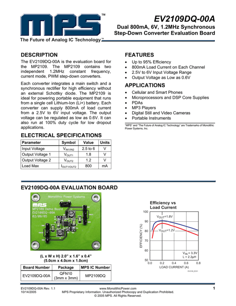
EV2109DQ-00A EVALUATION BOARD
Efficiency vs
Load Current
100
VOUT=1.8V
EFFICIENCY (%)
90
80
VOUT=1.2V
70
60
(L x W x H) 2.0” x 1.6” x 0.4”
(5.0cm x 4.0cm x 1.0cm)
Board Number
Package
QFN10
EV2109DQ-00A
(3mm x 3mm)
EV2109DQ-00A Rev. 1.1
10/14/2005
MPS IC Number
50
0.0
0.2
0.4
0.6
LOAD CURRENT (A)
0.8
EV2109_EC01
MP2109DQ
www.MonolithicPower.com
MPS Proprietary Information. Unauthorized Photocopy and Duplication Prohibited.
© 2005 MPS. All Rights Reserved.
1
TM
EV2109DQ-00A – DUAL 800mA, 6V, 1.2MHz SYNCHRONOUS STEP-DOWN CONVERTER
EVALUATION BOARD
EVALUATION BOARD SCHEMATIC
VOUT1
1.8V / 800mA
EN1
C5
NS
1
2
3
VIN
4
10
U1
EN1
SW1
FB1
GND
MP2109
IN2
IN1
FB2
GND
SW2
5
9
8
7
EN2
6
VOUT2
1.2V / 800mA
EN2
C6
NS
EV2109_S01
EV2109DQ-00A BILL OF MATERIALS
Qty
Ref
Value
Description
Package
Manufacturer
2
C1, C2
10µF
Ceramic Capacitor, 6.3V, X5R
1206
Any
2
C3, C4
22µF
Ceramic Capacitor, 6.3V, X5R
1206
Any
2
C5, C6
NS
2
L1, L2
SMD
Sumida
Do Not Stuff
2.2µH Inductor, 1.2A
0603
Any
2
R1, R3,
300kΩ Resistor, 1%
R4
R2
150kΩ Resistor, 1%
0603
Any
2
R5, R6
0603
Any
1
U1
QFN10
(3mm x 3mm)
MPS
3
100kΩ Resistor, 5%
EV2109DQ-00A Rev. 1.1
10/14/2005
Manufacturer P/N
DC-DC Converter
www.MonolithicPower.com
MPS Proprietary Information. Unauthorized Photocopy and Duplication Prohibited.
© 2005 MPS. All Rights Reserved.
CDRH3D16-2R2
MP2109DQ
2
TM
EV2109DQ-00A – DUAL 800mA, 6V, 1.2MHz SYNCHRONOUS STEP-DOWN CONVERTER
EVALUATION BOARD
PRINTED CIRCUIT BOARD LAYOUT
Figure 1—Top Silk Layer
Figure 2—Top Layer
Figure 3—Bottom Layer
EV2109DQ-00A Rev. 1.1
10/14/2005
www.MonolithicPower.com
MPS Proprietary Information. Unauthorized Photocopy and Duplication Prohibited.
© 2005 MPS. All Rights Reserved.
3
TM
EV2109DQ-00A – DUAL 800mA, 6V, 1.2MHz SYNCHRONOUS STEP-DOWN CONVERTER
EVALUATION BOARD
QUICK START GUIDE
The output voltages of this board are set to 1.8V (VOUT1) and 1.2V (VOUT2). The board layout
accommodates most commonly used inductors and output capacitors.
1. Attach the positive and negative ends of the first load to the VOUT1 and GND pins, respectively.
If using both outputs, attach the positive and negative ends of the second load to the VOUT2
and GND pins, respectively.
2. Attach the input voltage 2.5V ≤ VIN ≤ 6V and input ground to VIN and GND pins respectively.
3. A 100kΩ pull-up resistor has been connected to both the EN1 and EN2 pins, so both VOUT1
and VOUT2 will turn on without applying any external voltage to the EN1 and EN2 pins.
4. To turn on VOUT1/VOUT2 by using the EN1/EN2 functions, apply a voltage, 1.5V ≤ VEN1/EN2 ≤
6V, to the EN1/EN2 pin. To disable VOUT1/VOUT2, apply a voltage, VEN1/EN2 < 0.3V, to the
EN1/EN2 pin.
5. The output voltages VOUT1 and VOUT2 can be changed by varying R2 and R4, respectively.
Calculate the new values by the following formulae:
R2 =
R4 =
R1
⎛ VOUT1 ⎞
⎜⎜
⎟⎟ − 1
⎝ VFB ⎠
R3
⎛ VOUT 2
⎜⎜
⎝ VFB
⎞
⎟⎟ − 1
⎠
Where VFB = 0.6V, R1 = 300kΩ and R3 = 300kΩ.
Example:
For VOUT1 = 1.8V:
R2 =
300kΩ
= 150kΩ
⎛ 1.8 V ⎞
⎜
⎟ −1
⎝ 0 .6 V ⎠
Therefore, use a 150kΩ standard 1% value.
NOTICE: The information in this document is subject to change without notice. Please contact MPS for current specifications.
Users should warrant and guarantee that third party Intellectual Property rights are not infringed upon when integrating MPS
products into any application. MPS will not assume any legal responsibility for any said applications.
EV2109DQ-00A Rev. 1.1
10/14/2005
www.MonolithicPower.com
MPS Proprietary Information. Unauthorized Photocopy and Duplication Prohibited.
© 2005 MPS. All Rights Reserved.
4


