Product Specification
PE9309
3.0–13.5 GHz Low Power UltraCMOS®
Divide-by-4 Prescaler
Radiation Tolerant for Space
Applications
Product Description
he PE9309 is a high-performance dynamic UltraCMOS®
prescaler with a fixed divide ratio of 4. Its operating
frequency range is 3.0 GHz to 13.5 GHz. The PE9309
operates on a single supply with a frequency-selecting bias
resistor and draws only 16 mA. It is packaged in a small 8lead CFP and is also available in Die form for hybrid
application.
Features
High-frequency operation: up to 13.5 GHz
Fixed divide ratio of 4
Low-power operation:16 mA typical @
2.6V
Small package: 8-lead CFP
Available as DIE
The PE9309 is manufactured on Peregrine’s UltraCMOS
process, a patented variation of silicon-on-insulator (SOI)
technology on a sapphire substrate, offering the
performance of GaAs with the economy and integration of
conventional CMOS.
Figure 2. Package Type
8-lead CFP
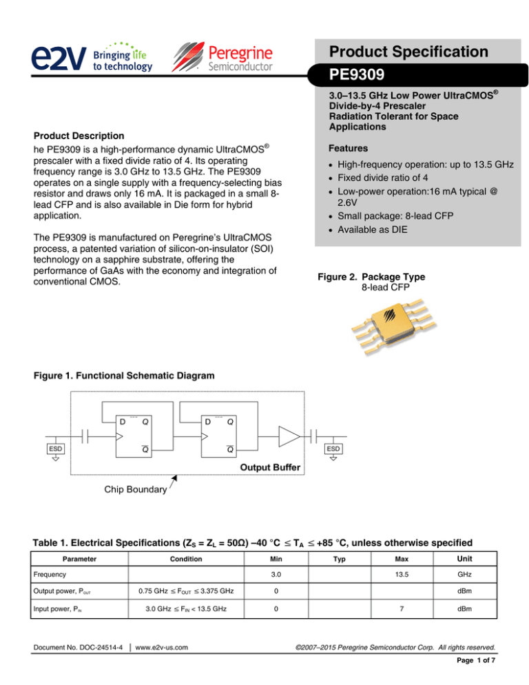
Figure 1. Functional Schematic Diagram
D
ESD
SET
CLR
D
Q
Q
SET
CLR
Q
ESD
Q
Output Buffer
Chip Boundary
Table 1. Electrical Specifications (ZS = ZL = 50Ω) –40 °C ≤ TA ≤ +85 °C, unless otherwise specified
Parameter
Condition
Frequency
Output power, POUT
Input power, PIN
Min
3.0
0.75 GHz ≤ FOUT ≤ 3.375 GHz
0
3.0 GHz ≤ FIN < 13.5 GHz
0
Document No. DOC-24514-4 │ www.e2v-us.com
Typ
Max
Unit
13.5
GHz
dBm
7
dBm
©2007–2015 Peregrine Semiconductor Corp. All rights reserved.
Page 1 of 7
PE9309
Product Specification
Table 4. Absolute Maximum Ratings
Figure 3. Pin Configuration (Top View)
Symbol
Pin 1 dot marking
VBYPS
1
8
RBIAS
VBYPS
2
7
VDD
9309
RF IN
3
GND
Top View
4
6
RF OUT
5
NC
Pin Name
Description
1
VBYPS
Prescaler supply bypass
2
VBYPS
Prescaler supply bypass
3
IN
RF input
4
GND
Ground
5
NC
6
OUT
RF output
7
VDD
Supply voltage
8
RBIAS
Frequency-selecting bias resistor
GND
GND
Bottom of the package is ground.
Connecting the bottom of the package to
ground is required
Unit
3.0
V
DC supply voltage
TST
Storage temperature range
–65
150
°C
TOP
Operating temperature
range
–40
85
°C
VESD
ESD voltage (Human Body
Model)
250
V
Maximum input power
14
dBm
Electrostatic Discharge (ESD) Precautions
When handling this UltraCMOS device, observe
the same precautions that you would use with
other ESD-sensitive devices. Although this device
contains circuitry to protect it from damage due to
ESD, precautions should be taken to avoid
exceeding the specified rating.
Not connected
Table 3. Operating Ranges
Latch-Up Immunity
Unlike conventional CMOS devices, UltraCMOS
devices are immune to latch-up.
ELDRS
Parameter
Min
Typ
Max
Unit
Supply voltage, VDD
2.45
2.6
2.75
V
Supply current, IDD
6
23
mA
©2007–2015 Peregrine Semiconductor Corp. All rights reserved.
Page 2 of 7
Max
Exceeding absolute maximum ratings may cause
permanent damage. Operation should be
restricted to the limits in the Operating Ranges
table. Operation between operating range
maximum and absolute maximum for extended
periods may reduce reliability.
GND
Table 2. Pin Descriptions
Pin #
Min
VDD
PIN_MAX
Side View
Parameter/Condition
UltraCMOS devices do not include bipolar minority
carrier elements, and therefore do no exhibit enhanced low dose rate sensitivity.
Document No. DOC-24514-4 │ UltraCMOS® RFIC Solutions
PE9309
Product Specification
Device Functional Considerations
The PE9309 divides a 3.0 GHz to 13.5 GHz input
signal by four, producing a 750 MHz to 3.375 GHz
output signal. In order for the prescaler to work
properly, several conditions need to be adhered to.
It is crucial that pins 1, 2 and 7 be supplied with
bypass capacitors to ground. In addition, the
output signal (pin 6) needs to be ac coupled via an
external capacitor as shown in the test circuit in
Figure 5.
The input frequency range is selected by the value
of RBIAS according to Figure 4.
The ground pattern on the board should be made
as wide as possible to minimize ground
impedance.
The bottom of the package is the primary ground
connection and it needs to be soldered to the PCB
ground.
Frequency (GHz)
Figure 4. Frequency vs RBIAS
15
14
Lower Freq Lim
13
12
Optimal Freq Lim
11
10
9
Upper Freq Lim
8
7
6
5
4
3
2
0
5
10
15
20
25
30
35
40
45
50
55
60
RBIAS (KOhm)
Document No. DOC-24514-4 │ www.e2v-us.com
©2007–2015 Peregrine Semiconductor Corp. All rights reserved.
Page 3 of 7
PE9309
Product Specification
Figure 5. Test Circuit Block Diagram
0.01μF
1
VBYPS
RBIAS 8
2
VBYPS
VDD
10 pF
10 pF
7
VDD
9309
3
50Ω
RBIAS
OUT
IN
6
T Line*
10 pF
4
GND
NC
0.01μF
5
Spectrum Analyzer
50Ω
6.8 pF
RF Source
T Line*
Side View
GND
*T Line = Transmission Line
Figure 6. High Frequency System Application
The wideband frequency of operation of the PE9309 makes it an ideal part for use in a DBS
down converter system.
INPUT
DBS 1
st
BPF
SAW
AGC
IF
FM
DEMOD
BASEBAND
OUTPUT
DIVIDE BY 4
PE97632
9309
LOW NOISE
PLL SYNTH
LPF
©2007–2015 Peregrine Semiconductor Corp. All rights reserved.
Page 4 of 7
Document No. DOC-24514-4 │ UltraCMOS® RFIC Solutions
PE9309
Product Specification
Figure 7. Evaluation Board Layouts
Evaluation Kit
The ceramic CFP prescaler evaluation board was
designed to help customers evaluate the PE9309
divide-by-4 prescaler. On this board, the device input
(pin 3) is connected to the SMA connector J5
through a 50Ω transmission line. The device output
(pin 6) is connected to SMA connector J6 through a
50Ω transmission line.
J4 provides DC power to the device via pin 7. J2
powers U2. Multiple decoupling capacitors (C4, 6,
13, 16 = 10pF, C3, 5, 14, 15 = 0.01uF) are used.
One out of eight different resistors for RBIAS is
selected by toggling SW1, SW2 and SW3 according
to the table shown in Figure 8. Jumper on J3 should
be on to lower setting (1 and 2). It is the
responsibility of the customer to determine proper
supply decoupling for their design application. The
board is constructed using 4 layers. The top and
bottom layers comprise Rogers low loss 4350
material having a core thickness of 0.010" while the
internal layers comprise FR-4. The overall board
thickness is 0.062".
PRT-17605
Figure 8. Evaluation Board Schematic
VDD 1
VDD2
Rbias
5.6K
8.2K
12.0K
18.0K
27.0K
39.0K
56.0K
82.0K
Hi Z
ADG708_16LEAD_TSSOP
J4
J3
1
HEADER 2
1
HEADER 2
+
+
C11
C8
10µF
10µF
2
2
1
2
1
A0
1
2
3
1
2
2
3
VDD1
R8
5.6K
4
R9
8.2K
5
R10
12.0K
6
18.0K
7
R1 1
A0
A1
EN
A2
VSS
GND
S1
VDD
S2
S5
S3
S6
S4
S7
D
S8
16
A1
15
A2
VDD1
14
R16
13
12
R12
11
R13
39.0K
10
R1 4
56.0K
9
R1 5
82.0K
0 OHM
27.0K
C5
C6
0.01uF
10pF
220
8
220
SW1
0
1
0
1
0
1
0
1
X
220
SW2
0
0
1
1
0
0
1
1
X
U2
VDD1
J2
SW3
0
0
0
0
1
1
1
1
X
C13
10pF
C14
0.01uF
VDD1
VDD2
4
3
2
1
DNI
6
4
R34
R33
6
DNI
R19
SW3
5
5
DNI
R18
R20
0 OHM
DNI
10
9
8
7
R24
DNI
R25
DNI
R26
DNI
A2
A1
A0
C3
C4
0.01uF
10pF
U1
Prescaler
6
2
3
4
5
R21
DNI
1
2
3
4
J5
R2
1
DNI
VBYPS RBIAS
VDD
VBYPS
OUT
IN
GND
NC
8
7
6
5
C15
C16
0.01uF
10pF
J6
C7
1
2
6.8pF
R3
R4
DNI
DNI
2
1
DNI
5
CA1
SW2
R22
SW1
J1
4
VDD1
6
4
R32
VDD1
R6
R5
DNI
DNI
R29
R28
2
10K
10K
D4
C9
C10
10pF
0.01uF
1
10K
DNI
R27
2
DNI
D3
1
1
D2
DNI
2
DOC-24526
VDD2
MT4
1
1
1
1
1
J8
1
2
MT3
2
MT2
50 OHM
J7
PCB MOUNTING HOLES
MT1
NOTES:
1. USE 101-0392-01 PCB
2. CAUTION:
CONTAINS PARTS AND ASSEMBLIES SUSCEPTIBLE
TO DAMAGEBY ELECTROSTATIC DISCHARGE (ESD)
3. ALL TRANSMISION LINES ARE:
35MIL WIDTH, 14MIL GAPS, 20MIL CORE DIELECTRIC
3.48 Er AND 2.8MIL Cu THICKNESS.
Document No. DOC-24514-4 │ www.e2v-us.com
©2007–2015 Peregrine Semiconductor Corp. All rights reserved.
Page 5 of 7
PE9309
Product Specification
Figure 9. Package Drawing
8-lead CFP
5.59-6.35
4.57 MAX
4.57 MAX
4.22
2.73
0.38±0.05
4.57 MAX 4.22 1.27
3.81
4.57 MAX
10.033±0.381
BOTTOM VIEW
TOP VIEW
2.73
0.25 Min
Lid
0.51
0.56
1.78 MAX
0.71
0.81 Min
0.25
0.51
0.254±0.05
0.32
MIN
0.127
1.70
MIN
DOC-50608
Side View
Figure 10. Top Marking Specifications
= Pin 1 indicator
●
9309-XX
YYWW
ZZZZZZZ
nnnnnn
PRT-17629
9309-XX = Part number (XX will be specified by the PO and/or
the assembly instructions)
YYWW = Date code, last two digits of the year and work week
ZZZZZZZ = Lot code (up to seven digits)
nnnnnn = Serial number of the part (up to six digits)
©2007–2015 Peregrine Semiconductor Corp. All rights reserved.
Page 6 of 7
Document No. DOC-24514-4 │ UltraCMOS® RFIC Solutions
PE9309
Product Specification
Table 5. Ordering Information
Order Code
Description
Package
Shipping Method
9309–01*
PE9309–08CFPJ–B Engineering samples
8-lead CFP
50 / Tray
9309–11
PE9309–08CFPJ–B Production units
8-lead CFP
50 / Tray
9309–00
PE9309 Evaluation kit
Evaluation kit
1 / Box
Note: * The 9309-01 devices are engineering sample (ES) prototype units intended for use as initial evaluation units for customers of the PE9309-11 flight units. The
PE9309-01 device provides the same functionality and footprint as the PE9309-11 space qualified device, and intended for engineering evaluation only. They are tested at
+25 °C only and processed to a non-compliant flow (e.g. no burn-in, non-hermetic, etc). These units are non-hermetic and are not suitable for qualification, production, radiation testing or flight use.
Sales Contact and Information
Contact Information:
e2v ~ http://www.e2v-us.com ~ inquiries@e2v-us.com
Advance Information: The product is in a formative or design stage. The datasheet contains design target
specifications for product development. Specifications and features may change in any manner without notice.
Preliminary Specification: The datasheet contains preliminary data. Additional data may be added at a later
date. Peregrine reserves the right to change specifications at any time without notice in order to supply the best
possible product. Product Specification: The datasheet contains final data. In the event Peregrine decides to
change the specifications, Peregrine will notify customers of the intended changes by issuing a CNF (Customer
Notification Form).
Document No. DOC-24514-4 │ www.e2v-us.com
The information in this datasheet is believed to be reliable. However, Peregrine assumes no liability for the use
of this information. Use shall be entirely at the user’s own risk.
No patent rights or licenses to any circuits described in this datasheet are implied or granted to any third party.
Peregrine’s products are not designed or intended for use in devices or systems intended for surgical implant,
or in other applications intended to support or sustain life, or in any application in which the failure of the
Peregrine product could create a situation in which personal injury or death might occur. Peregrine assumes no
liability for damages, including consequential or incidental damages, arising out of the use of its products in
such applications.
The Peregrine name, logo, UltraCMOS and UTSi are registered trademarks and HaRP, MultiSwitch and DuNE
are trademarks of Peregrine Semiconductor Corp. Peregrine products are protected under one or more of the
following U.S. Patents: http://patents.psemi.com.
©2007–2015 Peregrine Semiconductor Corp. All rights reserved.
Page 7 of 7


