Reverse-Biased PN Junctions • Theory of reverse pn
advertisement
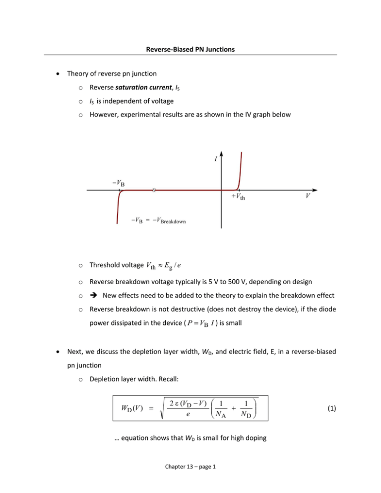
Reverse-Biased PN Junctions Theory of reverse pn junction o Reverse saturation current, IS o IS is independent of voltage o However, experimental results are as shown in the IV graph below o Threshold voltage Vth Eg / e o Reverse breakdown voltage typically is 5 V to 500 V, depending on design o New effects need to be added to the theory to explain the breakdown effect o Reverse breakdown is not destructive (does not destroy the device), if the diode power dissipated in the device ( P VB I ) is small Next, we discuss the depletion layer width, WD, and electric field, E, in a reverse-biased pn junction o Depletion layer width. Recall: WD (V ) 2 (VD V ) e 1 1 N N A D … equation shows that WD is small for high doping Chapter 13 – page 1 (1) o Maximum electric field. Recall: Ε max e N A x p0 (2) Also recall: x p0 ND WD NA ND (3) It follows from Eqns. (1) – (3) that Ε max 1 e 1 2 (VD V ) ND NA … Ε max increases for reverse bias Chapter 13 – page 2 1 (4) Zener effect (tunneling breakdown) “Tunneling” is a quantum mechanical effect o Classical mechanics versus quantum mechanics: A soccer ball with energy Eball Epot, barrier cannot get from one potential well to another one. An electron with kinetic energy Eelectron Epot, barrier can tunnel from one potential well to another one. If Ekin, ball Epot, ball Epot, wall , Then the ball will stay in the First well and cannot transfer to the second well. o Basis for quantum mechanical tunneling is Heisenberg’s uncertainty principle E t h (5) o If product of energy barrier height (E) and time required for tunneling (t) is sufficiently small, that is smaller than Planck’s constant h, then tunneling will occur. Tunnel barrier height E must be low for tunneling to occur. o If particle velocity = constant, then x t . Tunnel barrier thickness x must be thin for tunneling to occur. o Next, we apply this knowledge to a reverse-biased pn junction Chapter 13 – page 3 o Tunneling breakdown requires a large amount of filled states and a large amount of empty states separated by a potential barrier. Potential barrier must be low and narrow. 1 1 o Recall: WD NA ND o Tunnel distance x 1/ 2 Heavy doping makes potential barrier narrow 1 E max 1 V 1/ 2 o Tunneling breakdown will occur in lightly doped pn junctions at sufficiently high reverse voltages. Tunneling breakdown is called Zener breakdown. Such diodes are called Zener diodes. Typical Zener voltages = 5 – 20 V Chapter 13 – page 4 Avalanche breakdown Physical basis: Impact ionization at high electric fields. Generation of electron-hole pairs by impact ionization. o During impact ionization a rapidly propagating electrons hits the electron shell of an atom and “kicks” an electron out of its orbit thereby ionizing the atom o The free carriers created this way will create further free carriers by impact ionization carrier multiplication higher current o Band diagram: o Classical analogue: Snow avalanche … chain reaction o Avalanche breakdown occurs for … Large depletion layer thicknesses WD High electric fields Note that WD VD V 1 / 2 (V )1 / 2 E max VD V 1 / 2 (V )1 / 2 Also note that for high reverse voltages, it is VD V 1 / 2 V Chapter 13 – page 5 Exercise: o How would one design Zener diodes? Highly doped diodes o How would one design diodes with a high breakdown voltage? Lowly doped pn junctions Chapter 13 – page 6
