2016 1st International Electrical Engineering Congress (IEEC 2016)
May. 13-14, 2016 in IEP Centre, Karachi, Pakistan
Design of Advanced Neutral Point Clamped Multilevel Converter for AC Drive
Systems
M. Mansoor Alam1, Mumtaz Ahmad2, M. Asim Amin3, M. Ihsan Ul Haq4 and Attiq ur
Rehman5
1
School of Electrical Engineering, Xi'an Jiao Tong University, Xi'an Shaanxi, China
(mansoor.alam@pnec.nust.edu.pk)
2
School of Energy and Power Engineering, Xi'an Jiao Tong University, Xi'an
Shaanxi, China (mumtazqaisrani@yahoo.com)
3
School of Electrical Engineering, Xi'an Jiao Tong University, Xi'an Shaanxi, China
(masim.amin@yahoo.com)
4
National University of science and technology, (NUST), Pakistan (ihsanulhaq475@gmail.com)
5
School of Electrical Engineering, Xi'an Jiao Tong University, Xi'an Shaanxi, China (atnutkani@gmail.com)
Abstract: In recent years there has been augmenting progress related to multilevel converter designing. Inverters are
mainly composed of switching devices which produce output pulse width modulation (PWM) voltage on application of
suitable input modulation scheme. Having multilevel inverter has many advantages as compared to conventional PWM
schemes, the inverter includes less harmonic content if compared to conventional PWM type. Having multilevel, lessens
the voltage stress on the working switches insulated gate bipolar transistor (IGBT) which in effect reduces duration and
reduces voltage rating of switches. The advantages of neutral point clamped inverter not only limits at drive application
but expand to other industrial converter applications. Neutral clamping of the voltage and multilevel voltage output less
harmonic distortion less electromagnetic interference less deration of the motors due to decrease in the total harmonic
distortion (THD) of the system1. Providing twice the power output compared to other topologies and two-level inverter.
Having many advantages over previous multilevel converter topologies NPC stands out for drive implementation, and
power conversion purposes. In our research project we aim at developing converter which has multilevel converter
characteristics thus providing reduces total harmonic distortion, multilevel output , and improved power quality of output
waveform this will have far reaching effects on the industrial environment. Long lasting drive system improved efficiency.
Availability of large medium voltage converter system provide for driving of the large induction motors employed in
different machines such as induced fans , cooling fans and liquid pumps.
Keywords: Multilevel converter, total harmonic distortion, neutral point clamped, insulated gate bipolar transistor,
pulse width modulation.
I. INTRODUCTION
2) By developing a multilevel inverter
In recent few years, there have been a highly progress
towards the designing of converters. Many topologies
have been adopted. Some are AC to DC converter and
some are DC to AC converter2. We have adopted
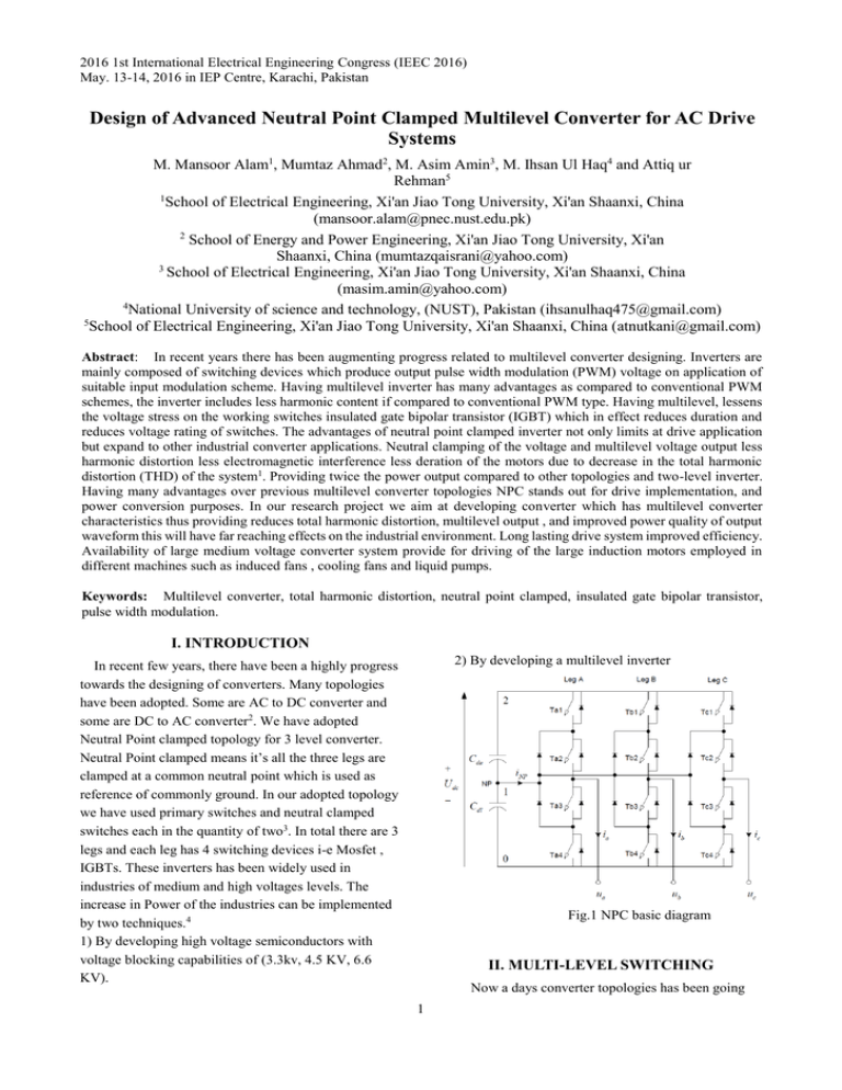
Neutral Point clamped topology for 3 level converter.
Neutral Point clamped means it’s all the three legs are
clamped at a common neutral point which is used as
reference of commonly ground. In our adopted topology
we have used primary switches and neutral clamped
switches each in the quantity of two3. In total there are 3
legs and each leg has 4 switching devices i-e Mosfet ,
IGBTs. These inverters has been widely used in
industries of medium and high voltages levels. The
increase in Power of the industries can be implemented
by two techniques.4
1) By developing high voltage semiconductors with
voltage blocking capabilities of (3.3kv, 4.5 KV, 6.6
KV).
Fig.1 NPC basic diagram
II. MULTI-LEVEL SWITCHING
Now a days converter topologies has been going
1
through modernization. Initially we have two level
inverters. They have high harmonics and (dv/dt) losses.
So we have adopted multilevel inverter topology. It has
less harmonics and less (dv/dt) losses, less switching
time. In our model Two capacitors are used to provide
the converter with voltage level of 0.5 VDC
independently. Consequently, if we allow the first two
switches to get on we get +0.5VDC given by 2 state.
and if we let on two middle switches we get neutral
voltage given by 1 state. And last two switches give the
-0.5vDC level.
Table.1 Switching sequence of our model
LEG
V1
T1
T2
T3
T4
VDC
VDC
0
ON
OFF
OFF
ON
ON
OFF
OFF
ON
ON
OFF
OFF
ON
STATE
2
1
0
III. Simulations
Simulations were made to check the progress of our
topology. Below is the figure of our simulations of
Neutral point clamped inverter with three legs. Each leg
has four switching devices which we can easily see in the
figure. Flying capacitors are also connected to provide
two different voltage level. So that commonly neutral
reference ground can be provided. In our project we have
made simulations of matlab and proteous software. Same
time to program the micro-controller we have used
Arduino. In the Fig 2 our matlab simulation. We have
three legs of semiconductor devices (IGBTs, Mosfet).
Each leg has 2 NPN and PNP are connected. Each leg is
connected with a commonly clamped neutral point
.
Fig.3 Vertical view of matlab simulation
IV. Results
From our simulations we have seen the fast switching
technique of our Neutral point clamped topology. In the
following figures we can check the matlab output.
Fig.2 a multi-level inverter output
In the above figure we can see that the output of
multilevel inverter is like stair case, in case of two level
converter we have square wave output. Which can cause
harmonic distortion in our machines. We use multi-level
inverter topology as its output waveform resembles a bit
more then sinusoidal as compared to that of square wave.
Fig.4 SPWM
2
As in Fig 4 it shows SPWM (sinusoidal pulse width
modulation) technique used for output of line to neutral
of all the three phases and also we can see the phase shift
in all phases. The three phases output waveform is nearly
related to our required sinusoidal rather than a square
waveform. We can check the different effects of our
waveform output by changing the load. As we can see in
the Fig 5 we have used an inductance of about 20mH.
The waveform has tips on the opposite side while zero
crossing point. Fig 5 shows the matlab waveforms of
signal output on all the three phases when we are using
inductance as our load. We can clearly observe the phase
shift in our result in each phase. In our matlab results we
can easily find out that our output has less distortion and
less (dv/dt) losses. In case of our inductive load, when
signal is positive the tip because of inductive load is in
negative side and also in case of negative signal top is in
positive side. Hence, our system will work accurate in
case of inductive load.
harmonic distortion will be more decreased. In case of
seven level voltage inverter we have total harmonic
distortion of about 10.7%.
An energy tank for the converter to which the control
circuit is expanded on for conversion to AC.
𝑉
𝐸𝑚 = 𝑑𝑐
(3)
𝑚−1
VDC= DC source voltage
Em= capacitor voltage
m= no of capacitor
V. CONCLUSION
From the simulations and results we have concluded that
it is very useful for medium voltage and high voltage
level industries as It can provide multilevel output of
(M+1) where M is the voltage levels. It produces output
with low electromagnetic interference. Three phases
share a common DC-bus minimizing the capacitance
requirements. The DC-link capacitors can be pre charged,
as a group. High efficiency for fundamental frequency
switching. Only three level NPC converter compared to
other converters can provide 2x the power output. NPC
can clamp the voltage to neutral. Thus avoiding the
floating voltage condition. The fundamental output
voltage is higher and better compared to other (two level).
Increased no of clamping diodes if many voltage levels
are required is the main drawback of this topology. But it
is the most cost effective topology till four (4) levels
compared to others.
Fig.5 Signal output with 20mH Inductance
Output of converters contain harmonics and power
quality of an inverter is evaluated on the basis of
following parameters.
Harmonic factor:
𝐻𝐹𝑛 =
𝑉𝑜𝑛
𝑉01
(1)
It is the measure of individual harmonic distribution.
Where V1 is rms valus of fundamental harmonic and Vn
is rms nth harmonic value.
Total harmonic distrortion:
For minimizing the effect of total harmonic distortion we
have to lower switching frequency. If THD is high we
face the deration of the motor or equipment under
operation and produces lower power quality of the
converter based system
∞
1
1
2
THD =
( ∑ Von
) .2
(2)
𝑉𝑜1
𝑛=2,3…
More voltage level output less will be total harmonic
distortion. In case of 2-level inverter we have a total
harmonic distortion of 48%, while in case of 5 level
inverter we have total harmonic distortion of 16.3%. if
we further increase the level of output voltage total
[1]
[2]
[3]
[4]
REFERENCES
Andreas nordvall , Multilevel inverter topology ,
Master of science thesis , Chalmers university of
technology, Goteborg , Sweden , 2011 , pg-13
Muhammad Haroon. Rashid , Power Electronics
circuits devices and applications , Third edition ,
Pearsons Prentice halls.
Luis Charlos Girlado Vasquez, Master of science
thesis , Norwegian university of science and
technology , june 2010.
Gobinath , Mahendra , Gnanmbal , New
Cascaded H-bridge multilevel inverter with
improved efficiency , dept of electrical and
electronics engineering , IJEIT , Vol 2 , issue 4 ,
April 2013.
