IL715/IL716/IL717
High Speed/High Temperature Four-Channel Digital Isolators
Functional Diagrams
Features
IN1
OUT1
IN2
OUT2
IN3
OUT3
IN4
OUT4
IL715
IN1
OUT1
IN2
OUT2
OUT3
IN3
OUT4
IN4
IL716
•
•
•
•
•
•
•
•
•
•
•
•
•
High speed: 110 Mbps
3 V to 5 V power supplies
High temperature: −40°C to +125°C (T-Series)
1.5 mA/channel typical quiescent current
100 ps typical pulse jitter
2 ns channel-to-channel skew
10 ns typical propagation delay
Low EMC footprint
30 kV/μs typical common mode transient immunity
44000 year barrier life
2500 VRMS isolation per UL 1577
UL 1577 recognized and IEC 61010-1 approved
0.3" and 0.15" 16-pin SOIC Packages
Applications
•
•
•
•
•
•
•
•
•
ADCs and DACs
Digital Fieldbus
Multiplexed data transmission
Board-to-board communication
Ground loop elimination
Parallel bus
Logic level shifting
Equipment covered under 61010-1 Edition 3
5 kVRMS rated IEC 60601-1 medical applications
Description
IN1
OUT1
IN2
OUT2
IN3
OUT3
OUT4
IN4
IL717
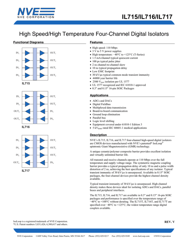
NVE’s IL715, IL716, and IL717 four-channel high-speed digital isolators
are CMOS devices manufactured with NVE’s patented* IsoLoop®
spintronic Giant Magnetoresistive (GMR) technology.
A unique ceramic/polymer composite barrier provides excellent isolation
and virtually unlimited barrier life.
All transmit and receive channels operate at 110 Mbps over the full
temperature and supply voltage range. The symmetric magnetic coupling
barrier provides a typical propagation delay of only 10 ns and a pulse width
distortion of 2 ns, achieving the best specifications of any isolator. Typical
transient immunity of 30 kV/µs is unsurpassed. Available in 0.15" SOIC
packages, the four-channel devices provide the highest channel density
available.
Typical transient immunity of 30 kV/µs is unsurpassed. High channel
density makes these devices ideal for isolating ADCs and DACs, parallel
buses and peripheral interfaces.
The IL715, IL716, and IL717 are available in 0.3" and 0.15" 16-pin SOIC
packages and performance is specified over the temperature range of
−40°C to +100°C without derating. The IL715T, IL716T, and IL717T are
specified over −40°C to +125°C; the widest temperature range digital
couplers available.
IsoLoop is a registered trademark of NVE Corporation.
*U.S. Patent numbers 5,831,426; 6,300,617 and others.
NVE Corporation
11409 Valley View Road, Eden Prairie, MN 55344-3617
REV. V
Phone: (952) 829-9217
Fax: (952) 829-9189
www.IsoLoop.com
©NVE Corporation
IL715/IL716/IL717
Absolute Maximum Ratings
Parameters
Storage Temperature
Ambient Operating Temperature(1)
IL715T, IL716T, and IL717T
Supply Voltage
Input Voltage
Output Voltage
Output Current Drive
Lead Solder Temperature
ESD
Symbol
TS
Min.
−55
TA
−40
VDD1, VDD2
VI
VO
IO
−0.5
−0.5
−0.5
Typ.
Max.
150
100
125
7
VDD+0.5
VDD+0.5
10
260
Units
°C
Max.
Units
100
125
5.5
VDD
0.8
1
°C
°C
V
V
V
µs
Max.
Units
2
Test Conditions
°C
V
V
V
mA
°C
kV
10 sec.
HBM
Recommended Operating Conditions
Parameters
Ambient Operating Temperature
IL715, IL716, and IL717
IL715T, IL716T, and IL717T
Supply Voltage
Logic High Input Voltage
Logic Low Input Voltage
Input Signal Rise and Fall Times
Symbol
Min.
TA
TA
VDD1, VDD2
VIH
VIL
tIR, tIF
−40
−40
3.0
2.4
0
Symbol
Min.
4.03
8.08
0.012
Typ.
Test Conditions
Insulation Specifications
Parameters
Creepage Distance 0.15" SOIC
(external)
0.3" SOIC
Total Barrier Thickness (internal)
Leakage Current(5)
Barrier Impedance(5)
Typ.
Test Conditions
mm
0.013
0.2
>1014||3
Barrier Life
mm
µA
Ω || pF
Years at
100°C
44000
240 VRMS, 60 Hz
60% confidence level
activation energy
Package Characteristics
Parameters
Capacitance (Input–Output)(5)
Thermal Resistance
0.15" SOIC
0.3" SOIC
Package Power Dissipation
Symbol
CI–O
Min.
Typ.
4
θJC
θJC
Max.
41
28
150
PPD
Units
pF
Test Conditions
f = 1 MHz
°C/W
°C/W
mW
Thermocouple at center
underside of package
f = 1 MHz, VDD = 5 V
Safety and Approvals
IEC61010-1
TUV Certificate Numbers:
N1502812, N1502812-101
Classification as reinforced insulation:
Model
IL715, IL716, and IL717
IL715-3, IL716-3, and IL717-3
Package
0.3" SOIC
0.15" SOIC
Pollution Degree
II
II
Material Group
III
III
Max. Working
Voltage
300 VRMS
150 VRMS
UL 1577
Component Recognition Program File Number: E207481
Each part tested at 3000 VRMS (4240 VPK) for 1 second
Each lot sample tested at 2500 VRMS (3530 VPK) for 1 minute
Soldering Profile
Per JEDEC J-STD-020C, MSL=2
2
NVE Corporation
11409 Valley View Road, Eden Prairie, MN 55344-3617
Phone: (952) 829-9217
Fax: (952) 829-9189
www.IsoLoop.com
©NVE Corporation
IL715/IL716/IL717
IL715 Pin Connections
1
2
3
4
5
6
7
8
9
10
11
12
13
14
15
16
VDD1
GND1
IN1
IN2
IN3
IN4
NC
GND1
GND2
NC
OUT4
OUT3
OUT2
OUT1
GND2
VDD2
Supply voltage
Ground return for VDD1*
Data in, channel 1
Data in, channel 2
Data in, channel 3
Data in, channel 4
No connection
Ground return for VDD1*
Ground return for VDD2*
No connection
Data out, channel 4
Data out, channel 3
Data out, channel 2
Data out, channel 1
Ground return for VDD2*
Supply voltage
VDD1
VDD2
GND1
GND2
IN1
OUT1
IN2
OUT2
IN3
OUT3
IN4
OUT4
NC
NC
GND2
GND1
IL715
IL716 Pin Connections
1
2
3
4
5
6
7
8
9
10
11
12
13
14
15
16
VDD1
GND1
IN1
IN2
OUT3
OUT4
NC
GND1
GND2
NC
IN4
IN3
OUT2
OUT1
GND2
VDD2
Supply voltage
Ground Return for VDD1*
Data in, channel 1
Data in, channel 2
Data out, channel 3
Data out, channel 4
No connection
Ground Return for VDD1*
Ground Return for VDD2*
No connection
Data in, channel 4
Data in, channel 3
Data out, channel 2
Data out, channel 1
Ground Return for VDD2*
Supply voltage
VDD1
VDD2
GND1
GND2
IN1
OUT1
IN2
OUT2
OUT3
IN3
OUT4
IN4
NC
NC
GND2
GND1
IL716
*NOTE: Pins 2 and 8 are internally connected, as are pins 9 and 15.
3
NVE Corporation
11409 Valley View Road, Eden Prairie, MN 55344-3617
Phone: (952) 829-9217
Fax: (952) 829-9189
www.IsoLoop.com
©NVE Corporation
IL715/IL716/IL717
IL717 Pin Connections
1
2
3
4
5
6
7
8
9
10
11
12
13
14
15
16
VDD1
GND1
IN1
IN2
IN3
OUT4
NC
GND1
GND2
NC
IN4
OUT3
OUT2
OUT1
GND2
VDD2
Supply voltage
Ground return for VDD1*
Data in, channel 1
Data in, channel 2
Data in, channel 3
Data out, channel 4
No connection
Ground return for VDD1*
Ground return for VDD2*
No connection
Data in, channel 4
Data out, channel 3
Data out, channel 2
Data out, channel 1
Ground return for VDD2*
Supply voltage
VDD1
VDD2
GND1
GND2
IN1
OUT1
IN2
OUT2
IN3
OUT3
OUT4
IN4
NC
NC
GND2
GND1
IL717
*NOTE: Pins 2 and 8 are internally connected, as are pins 9 and 15.
Timing Diagram
Legend
tPLH
tPHL
tPW
tR
tF
Propagation Delay, Low to High
Propagation Delay, High to Low
Minimum Pulse Width
Rise Time
Fall Time
4
NVE Corporation
11409 Valley View Road, Eden Prairie, MN 55344-3617
Phone: (952) 829-9217
Fax: (952) 829-9189
www.IsoLoop.com
©NVE Corporation
IL715/IL716/IL717
Parameters
Input Quiescent Supply Current
IL715
IL716
IL717
Output Quiescent Supply Current
IL715
IL716
IL717
Logic Input Current
3.3 Volt Electrical Specifications (Tmin to Tmax unless otherwise stated)
Symbol
Min.
Typ.
Max.
Units
IDD1
16
3
1.5
20
4
2
µA
mA
mA
IDD2
6
3
4.5
8
4
6
10
mA
mA
mA
µA
II
Logic High Output Voltage
VOH
Logic Low Output Voltage
VOL
Maximum Data Rate
Pulse Width(7)
Propagation Delay Input to Output
(High to Low)
Propagation Delay Input to Output
(Low to High)
Pulse Width Distortion (2)
Propagation Delay Skew (3)
Output Rise Time (10%−90%)
Output Fall Time (10%−90%)
Common Mode Transient Immunity
(Output Logic High or Logic Low)(4)
Channel-to-Channel Skew
Dynamic Power Consumption(6)
Power Frequency Magnetic Immunity
Pulse Magnetic Field Immunity
Damped Oscillatory Magnetic Field
Cross-axis Immunity Multiplier(9)
−10
VDD − 0.1
0.8 x VDD
VDD
0.9 x VDD
0
0.5
V
0.1
0.8
Switching Specifications (VDD = 3.3 V)
100
110
PW
10
V
Mbps
ns
Test Conditions
IO = −20 µA, VI = VIH
IO = −4 mA, VI = VIH
IO = 20 µA, VI = VIL
IO = 4 mA, VI = VIL
CL = 15 pF
50% Points, VO
tPHL
12
18
ns
CL = 15 pF
tPLH
12
18
ns
CL = 15 pF
PWD
tPSK
tR
tF
2
4
2
2
3
6
4
4
ns
ns
ns
ns
CL = 15 pF
CL = 15 pF
CL = 15 pF
CL = 15 pF
|CMH|,|CML|
20
30
tCSK
2
140
3
240
Magnetic Field Immunity(8) (VDD2 = 3V, 3V <VDD1 <5.5V)
HPF
1000
1500
HPM
1800
2000
HOSC
1800
2000
KX
2.5
kV/µs
VCM = 300 V
ns
μA/MHz
CL = 15 pF
per channel
A/m
A/m
A/m
50Hz/60Hz
tp = 8µs
0.1Hz – 1MHz
5
NVE Corporation
11409 Valley View Road, Eden Prairie, MN 55344-3617
Phone: (952) 829-9217
Fax: (952) 829-9189
www.IsoLoop.com
©NVE Corporation
IL715/IL716/IL717
Parameters
Input Quiescent Supply Current
IL715
IL716
IL717
Output Quiescent Supply Current
IL715
IL716
IL717
Logic Input Current
5 Volt Electrical Specifications (Tmin to Tmax unless otherwise stated)
Symbol
Min.
Typ.
Max.
Units
IDD1
24
4
2
30
6
3
µA
mA
mA
IDD2
8
4
6
12
6
9
10
mA
mA
mA
µA
II
Logic High Output Voltage
VOH
Logic Low Output Voltage
VOL
Maximum Data Rate
Pulse Width(7)
Propagation Delay Input to Output
(High to Low)
Propagation Delay Input to Output
(Low to High)
Pulse Width Distortion(2)
Pulse Jitter(10)
Propagation Delay Skew(3)
Output Rise Time (10%−90%)
Output Fall Time (10%−90%)
Common Mode Transient Immunity
(Output Logic High or Logic Low)(4)
Channel-to-Channel Skew
Dynamic Power Consumption(6)
Power Frequency Magnetic Immunity
Pulse Magnetic Field Immunity
Damped Oscillatory Magnetic Field
Cross-axis Immunity Multiplier(9)
−10
VDD − 0.1
0.8 x VDD
VDD
0.9 x VDD
0
0.5
V
0.1
0.8
Switching Specifications (VDD = 5V)
100
110
PW
10
V
Mbps
ns
Test Conditions
IO = −20 µA, VI = VIH
IO = −4 mA, VI = VIH
IO = 20 µA, VI = VIL
IO = 4 mA, VI = VIL
CL = 15 pF
50% Points, VO
tPHL
10
15
ns
CL = 15 pF
tPLH
10
15
ns
CL = 15 pF
PWD
tJ
tPSK
tR
tF
2
100
4
1
1
3
ps
ns
ns
ns
CL = 15 pF
CL = 15 pF
CL = 15 pF
CL = 15 pF
CL = 15 pF
|CMH|,|CML|
20
6
3
3
30
tCSK
2
200
3
340
Magnetic Field Immunity(8) (VDD2= 5V, 3V<VDD1<5.5V)
HPF
2800
3500
HPM
4000
4500
HOSC
4000
4500
KX
2.5
kV/µs
Vcm = 300 V
ns
μA/MHz
CL = 15 pF
per channel
A/m
A/m
A/m
50Hz/60Hz
tp = 8µs
0.1Hz – 1MHz
Notes (apply to both 3.3 V and 5 V specifications):
1.
Absolute maximum ambient operating temperature means the device will not be damaged if operated under these conditions. It does not
guarantee performance.
2.
PWD is defined as |tPHL − tPLH|. %PWD is equal to PWD divided by pulse width.
3.
tPSK is the magnitude of the worst-case difference in tPHL and/or tPLH between devices at 25°C.
4.
CMH is the maximum common mode voltage slew rate that can be sustained while maintaining VO > 0.8 VDD2. CML is the maximum
common mode input voltage that can be sustained while maintaining VO < 0.8 V. The common mode voltage slew rates apply to both rising
and falling common mode voltage edges.
5.
Device is considered a two terminal device: pins 1–8 shorted and pins 9–16 shorted.
6.
Dynamic power consumption is calculated per channel and is supplied by the channel’s input side power supply.
7.
Minimum pulse width is the minimum value at which specified PWD is guaranteed.
8.
The relevant test and measurement methods are given in the Electromagnetic Compatibility section on p. 7.
9.
External magnetic field immunity is improved by this factor if the field direction is “end-to-end” rather than to “pin-to-pin” (see diagram on p. 7).
10. 66,535-bit pseudo-random binary signal (PRBS) NRZ bit pattern with no more than five consecutive 1s or 0s; 800 ps transition time.
6
NVE Corporation
11409 Valley View Road, Eden Prairie, MN 55344-3617
Phone: (952) 829-9217
Fax: (952) 829-9189
www.IsoLoop.com
©NVE Corporation
IL715/IL716/IL717
Application Information
Electrostatic Discharge Sensitivity
Power Supply Decoupling
This product has been tested for electrostatic sensitivity to the
limits stated in the specifications. However, NVE recommends that
all integrated circuits be handled with appropriate care to avoid
damage. Damage caused by inappropriate handling or storage could
range from performance degradation to complete failure.
Both power supplies to these devices should be decoupled with low
ESR 47 nF ceramic capacitors. Ground planes for both GND1 and
GND2 are highly recommended for data rates above 10 Mbps.
Capacitors must be located as close as possible to the VDD pins.
Signal Status on Start-up and Shut Down
Electromagnetic Compatibility
To minimize power dissipation, input signals are differentiated and
then latched on the output side of the isolation barrier to reconstruct
the signal. This could result in an ambiguous output state
depending on power up, shutdown and power loss sequencing.
Therefore, the designer should consider including an initialization
signal in the start-up circuit. Initialization consists of toggling the
input either high then low, or low then high.
IsoLoop Isolators have the lowest EMC footprint of any isolation
technology. IsoLoop Isolators’ Wheatstone bridge configuration
and differential magnetic field signaling ensure excellent EMC
performance against all relevant standards.
These isolators are fully compliant with generic EMC standards
EN50081, EN50082-1 and the umbrella line-voltage standard for
Information Technology Equipment (ITE) EN61000. NVE has
completed compliance tests in the categories below:
Data Transmission Rates
The reliability of a transmission system is directly related to the
accuracy and quality of the transmitted digital information. For a
digital system, those parameters which determine the limits of the
data transmission are pulse width distortion and propagation delay
skew.
EN50081-1
Residential, Commercial & Light Industrial
Methods EN55022, EN55014
EN50082-2: Industrial Environment
Methods EN61000-4-2 (ESD), EN61000-4-3 (Electromagnetic
Field Immunity), EN61000-4-4 (Electrical Transient Immunity),
EN61000-4-6 (RFI Immunity), EN61000-4-8 (Power Frequency
Magnetic Field Immunity), EN61000-4-9 (Pulsed Magnetic
Field), EN61000-4-10 (Damped Oscillatory Magnetic Field)
ENV50204
Radiated Field from Digital Telephones (Immunity Test)
Propagation delay is the time taken for the signal to travel through
the device. This is usually different when sending a low-to-high
than when sending a high-to-low signal. This difference, or error, is
called pulse width distortion (PWD) and is usually in nanoseconds.
It may also be expressed as a percentage:
PWD% = Maximum Pulse Width Distortion (ns)
Signal Pulse Width (ns)
Immunity to external magnetic fields is even higher if the field
direction is “end-to-end” rather than to “pin-to-pin” as shown in the
diagram below:
x 100%
For example, with data rates of 12.5 Mbps:
PWD% = 3 ns x 100% = 3.75%
80 ns
This figure is almost three times better than any available
optocoupler with the same temperature range, and two times better
than any optocoupler regardless of published temperature range.
IsoLoop isolators exceed the 10% maximum PWD recommended
by PROFIBUS, and will run to nearly 35 Mb within the 10% limit.
Cross-axis Field Direction
Propagation delay skew is the signal propagation difference
between two or more channels. This becomes significant in clocked
systems because it is undesirable for the clock pulse to arrive
before the data has settled. Short propagation delay skew is
therefore especially critical in high data rate parallel systems for
establishing and maintaining accuracy and repeatability. Worstcase channel-to-channel skew in an IL700 Isolator is only 3 ns,
which is ten times better than any optocoupler. IL700 Isolators
have a maximum propagation delay skew of 6 ns, which is five
times better than any optocoupler.
Dynamic Power Consumption
IsoLoop Isolators achieve their low power consumption from the
way they transmit data across the isolation barrier. By detecting the
edge transitions of the input logic signal and converting these to
narrow current pulses, a magnetic field is created around the GMR
Wheatstone bridge. Depending on the direction of the magnetic
field, the bridge causes the output comparator to switch following
the input logic signal. Since the current pulses are narrow, about
2.5 ns, the power consumption is independent of mark-to-space
ratio and solely dependent on frequency. This has obvious
advantages over optocouplers, which have power consumption
heavily dependent on mark-to-space ratio.
7
NVE Corporation
11409 Valley View Road, Eden Prairie, MN 55344-3617
Phone: (952) 829-9217
Fax: (952) 829-9189
www.IsoLoop.com
©NVE Corporation
IL715/IL716/IL717
Application Diagrams
Isolated Logic Level Shifters
+5V
+3.3V
DO
DI
Sensor
Controller
ADC
CLK
CS
IL717
GND 1
GND 2
Single-Channel Isolated Delta-Sigma A/D Converter
Bridge
Bias
Delta Sigma A/D
CS5532
Bridge +
Bridge Isolation
Boundary
Serial Data Out
Iso SD Out
Serial Data In
Iso SD In
Data Clock
Iso Data Clock
Chip Select
Iso CS
IL717
Clock
Generator
OSC 2
This circuit illustrates a typical single-channel delta-sigma ADC. The A/D is located on the bridge with no signal conditioning electronics
between the bridge sensor and the ADC. In this case, the IL717 is the best choice for isolation. It isolates the control bus from the
microcontroller. The system clock is located on the isolated side of the system.
8
NVE Corporation
11409 Valley View Road, Eden Prairie, MN 55344-3617
Phone: (952) 829-9217
Fax: (952) 829-9189
www.IsoLoop.com
©NVE Corporation
IL715/IL716/IL717
Package Drawings, Dimensions and Specifications
0.15" SOIC Package
Dimensions in inches (mm)
0.152 (3.86)
0.157 (3.99)
0.013 (0.3)
0.020 (0.5)
NOM
0.016 (0.4)
0.050 (1.3)
0.007 (0.2)
0.013 (0.3)
0.386 (9.8)
0.394 (10.0)
Pin 1 identified
by either an
indent or a
marked dot
0.228 (5.8)
0.244 (6.2)
0.054 (1.4)
0.072 (1.8)
0.040 (1.02)
0.050 (1.27)
0.040 (1.0)
NOTE: Pin spacing is a BASIC 0.060 (1.5)
dimension; tolerances
do not accumulate
0.004 (0.1)
0.012 (0.3)
0.3" SOIC Package
Dimensions in inches (mm)
0.287 (7.29)
0.300 (7.62)
0.013 (0.3)
0.020 (0.5)
NOM
0.016 (0.4)
0.050 (1.3)
0.007 (0.2)
0.013 (0.3)
0.397 (10.1)
0.413 (10.5)
Pin 1 identified by
either an indent
or a marked dot
0.394 (10.00)
0.419 (10.64)
0.092 (2.34)
0.105 (2.67)
0.08 (2.0)
0.10 (2.5)
0.040 (1.0)
NOTE: Pin spacing is a BASIC 0.060 (1.5)
dimension; tolerances
do not accumulate
0.004 (0.1)
0.012 (0.3)
9
NVE Corporation
11409 Valley View Road, Eden Prairie, MN 55344-3617
Phone: (952) 829-9217
Fax: (952) 829-9189
www.IsoLoop.com
©NVE Corporation
IL715/IL716/IL717
Ordering Information and Valid Part Numbers
IL 716 T - 3 E TR13
Valid Part Numbers
Bulk Packaging
Blank = Tube
TR7 = 7'' Tape and Reel
TR13 = 13'' Tape and Reel
Package
Blank = 80/20 Tin/Lead Plating
E = RoHS Compliant
Package Type
Blank = 0.30'' 16-pin SOIC
-3 = 0.15'' 16-pin SOIC
IL715
IL715E
IL715-3
IL715-3E
IL715T
IL715TE
IL715T-3
IL715T-3E
IL716
IL716E
IL716-3
IL716-3E
IL716T
IL716TE
IL716T-3
IL716T-3E
IL717
IL717E
IL717-3
IL717-3E
IL717T
IL717TE
IL717T-3
IL717T-3E
All IL715, IL716, and IL717 part types are
available on tape and reel.
Grade
Blank = Standard Temp.
T = High Temperature
Base Part Number
715 = 4 Drive Channels
716 = 2 Drive Channels
2 Receive Channels
717 = 3 Drive Channels
1 Receive Channel
Product Family
IL = Isolators
RoHS
COMPLIANT
10
NVE Corporation
11409 Valley View Road, Eden Prairie, MN 55344-3617
Phone: (952) 829-9217
Fax: (952) 829-9189
www.IsoLoop.com
©NVE Corporation
IL715/IL716/IL717
ISB-DS-001-IL715/6/7-V
December 2012
ISB-DS-001-IL715/6/7-U
ISB-DS-001-IL715/6/7-T
ISB-DS-001-IL715/6/7-S
ISB-DS-001-IL715/6/7-R
ISB-DS-001-IL715/6/7-Q
ISB-DS-001-IL715/6/7-P
Changes
•
Detailed isolation and barrier specifications.
•
Cosmetic changes.
Changes
•
Tightened typical output quiescent supply spec. to 1.5 mA/channel at 3.3V.
Changes
•
Updates to terms and conditions.
Changes
•
Added clarification of internal ground connections (pp. 3-4).
Changes
•
Added typical jitter specification at 5V.
Changes
•
Added EMC details.
Changes
•
Added magnetic field immunity and electromagnetic compatibility specifications.
•
Added notes on package drawings that pin-spacing tolerances are non-accumulating.
ISB-DS-001-IL715/6/7-O
Changes
• Changed ordering information to reflect that devices are now fully RoHS compliant
with no exemptions.
ISB-DS-001-IL715/6/7-N
Changes
• Eliminated soldering profile chart
ISB-DS-001-IL715/6/7-M
Changes
• Package drawings updated
ISB-DS-001-IL715/6/7-L
Changes
• T-Grades added
ISB-DS-001-IL715/6/7-K
•
Package drawings updated
•
Order information updated
Changes
• Update UL and IEC approvals
•
Package characteristics added
11
NVE Corporation
11409 Valley View Road, Eden Prairie, MN 55344-3617
Phone: (952) 829-9217
Fax: (952) 829-9189
www.IsoLoop.com
©NVE Corporation
IL715/IL716/IL717
Datasheet Limitations
The information and data provided in datasheets shall define the specification of the product as agreed between NVE and its customer, unless NVE and
customer have explicitly agreed otherwise in writing. All specifications are based on NVE test protocols. In no event however, shall an agreement be
valid in which the NVE product is deemed to offer functions and qualities beyond those described in the datasheet.
Limited Warranty and Liability
Information in this document is believed to be accurate and reliable. However, NVE does not give any representations or warranties, expressed or
implied, as to the accuracy or completeness of such information and shall have no liability for the consequences of use of such information.
In no event shall NVE be liable for any indirect, incidental, punitive, special or consequential damages (including, without limitation, lost profits, lost
savings, business interruption, costs related to the removal or replacement of any products or rework charges) whether or not such damages are based on
tort (including negligence), warranty, breach of contract or any other legal theory.
Right to Make Changes
NVE reserves the right to make changes to information published in this document including, without limitation, specifications and product descriptions
at any time and without notice. This document supersedes and replaces all information supplied prior to its publication.
Use in Life-Critical or Safety-Critical Applications
Unless NVE and a customer explicitly agree otherwise in writing, NVE products are not designed, authorized or warranted to be suitable for use in life
support, life-critical or safety-critical devices or equipment. NVE accepts no liability for inclusion or use of NVE products in such applications and such
inclusion or use is at the customer’s own risk. Should the customer use NVE products for such application whether authorized by NVE or not, the
customer shall indemnify and hold NVE harmless against all claims and damages.
Applications
Applications described in this datasheet are illustrative only. NVE makes no representation or warranty that such applications will be suitable for the
specified use without further testing or modification.
Customers are responsible for the design and operation of their applications and products using NVE products, and NVE accepts no liability for any
assistance with applications or customer product design. It is customer’s sole responsibility to determine whether the NVE product is suitable and fit for
the customer’s applications and products planned, as well as for the planned application and use of customer’s third party customers. Customers should
provide appropriate design and operating safeguards to minimize the risks associated with their applications and products.
NVE does not accept any liability related to any default, damage, costs or problem which is based on any weakness or default in the customer’s
applications or products, or the application or use by customer’s third party customers. The customer is responsible for all necessary testing for the
customer’s applications and products using NVE products in order to avoid a default of the applications and the products or of the application or use by
customer’s third party customers. NVE accepts no liability in this respect.
Limiting Values
Stress above one or more limiting values (as defined in the Absolute Maximum Ratings System of IEC 60134) will cause permanent damage to the
device. Limiting values are stress ratings only and operation of the device at these or any other conditions above those given in the recommended
operating conditions of the datasheet is not warranted. Constant or repeated exposure to limiting values will permanently and irreversibly affect the
quality and reliability of the device.
Terms and Conditions of Sale
In case an individual agreement is concluded only the terms and conditions of the respective agreement shall apply. NVE hereby expressly objects to
applying the customer’s general terms and conditions with regard to the purchase of NVE products by customer.
No Offer to Sell or License
Nothing in this document may be interpreted or construed as an offer to sell products that is open for acceptance or the grant, conveyance or implication
of any license under any copyrights, patents or other industrial or intellectual property rights.
Export Control
This document as well as the items described herein may be subject to export control regulations. Export might require a prior authorization from national
authorities.
Automotive Qualified Products
Unless the datasheet expressly states that a specific NVE product is automotive qualified, the product is not suitable for automotive use. It is neither
qualified nor tested in accordance with automotive testing or application requirements. NVE accepts no liability for inclusion or use of non-automotive
qualified products in automotive equipment or applications.
In the event that customer uses the product for design-in and use in automotive applications to automotive specifications and standards, customer (a) shall
use the product without NVE’s warranty of the product for such automotive applications, use and specifications, and (b) whenever customer uses the
product for automotive applications beyond NVE’s specifications such use shall be solely at customer’s own risk, and (c) customer fully indemnifies
NVE for any liability, damages or failed product claims resulting from customer design and use of the product for automotive applications beyond NVE’s
standard warranty and NVE’s product specifications.
12
NVE Corporation
11409 Valley View Road, Eden Prairie, MN 55344-3617
Phone: (952) 829-9217
Fax: (952) 829-9189
www.IsoLoop.com
©NVE Corporation
IL715/IL716/IL717
An ISO 9001 Certified Company
NVE Corporation
11409 Valley View Road
Eden Prairie, MN 55344-3617 USA
Telephone: (952) 829-9217
Fax: (952) 829-9189
www.nve.com
e-mail: iso-info@nve.com
©NVE Corporation
All rights are reserved. Reproduction in whole or in part is prohibited without the prior written consent of the copyright owner.
ISB-DS-001-IL715/6/7-V
December 2012
13
NVE Corporation
11409 Valley View Road, Eden Prairie, MN 55344-3617
Phone: (952) 829-9217
Fax: (952) 829-9189
www.IsoLoop.com
©NVE Corporation
