Inverters - benchmark
advertisement
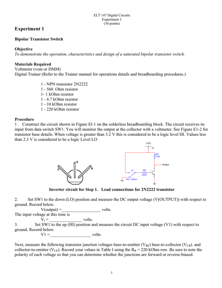
ELT 147 Digital Circuits Experiment 1 (10 points) Experiment 1 Bipolar Transistor Switch Objective To demonstrate the operation, characteristics and design of a saturated bipolar transistor switch. Materials Required Voltmeter (vom or DMM) Digital Trainer (Refer to the Trainer manual for operations details and breadboarding procedures.) 1 - NPN transistor 2N2222 1 - 560 Ohm resistor 1- 1 kOhm resistor 1 - 4.7 kOhm resistor 1 - 10 kOhm resistor 1 - 220 kOhm resistor Procedure 1 . Construct the circuit shown in Figure El-1 on the solderless breadboarding block. The circuit receives its input from data switch SW1. You will monitor the output at the collector with a voltmeter. See Figure E1-2 for transistor base details. When voltage is greater than 3.2 V this is considered to be a logic level HI. Values less than 2.3 V is considered to be a logic Level LO VCC 5V R1 1.0kΩ Output J1 R2 220kΩ C B E Key = Space Inverter circuit for Step 1. Lead connections for 2N2222 transistor 2. Set SW1 to the down (LO) position and measure the DC output voltage (V(OUTPUT)) with respect to ground. Record below. V(output) =__________________ volts. The input voltage at this time is VI = _______________ volts. 3. Set SW1 to the up (HI) position and measure the circuit DC input voltage (V1) with respect to ground. Record below. V1 =___________________ volts. Next, measure the following transistor junction voltages base-to-emitter (VBE) base-to-collector (VCB). and collector-to-emitter (VCE). Record your values in Table I using the RB = 220 kOhm row. Be sure to note the polarity of each voltage so that you can determine whether the junctions are forward or reverse-biased. 1 ELT 147 Digital Circuits Experiment 1 (10 points) RB VBE VCB TABLE I VCE=V(OUTPUT) Is the transistor Saturated 220KOhm 4.7KOhm 4. Turn on Switch 1. easure the voltage drop across the 220 kOhm base resistor (VRB) and the voltage across the collector resistor (VRC) and record in Table II in the RB = 220 kOhm column. Using these voltages and associated resistor values, calculate the base current (IB.) and collector current (IC) using Ohm's law. V IB = RB RB IC = VRC RC Record your values in Table II. Also calculate the ratio V. and record in Table II. TABLE II RB=4.7KOhm RB=220KOhm VRB VRC IB IC IC/IB 5. Using the criterion that states a transistor is saturated if the IC/IB < hFE, and the data in Table II, determine the condition of the transistor assuming hFE = 100. Is the transistor saturated? ____________________________ 6. Replace the 220 kOhm base resistor R. with a 4.7 kOhm resistor. 7. Repeat Step 3. Measure VBE, Vc and VcE and record in Table 1. Study your results. 8. Repeat Step 4 recording your data in Table II. 9. Repeat Step 5. Is the transistor saturated? _________________ 2 ELT 147 Digital Circuits Experiment 1 (10 points) Experiment 2 Logic Inverter Objective To demonstrate the operation and characteristics of typical discrete component and integrated circuit logic inverters. Materials Required DC Voltmeter 2 - 2N2222 transistor 2 -1 kOhm resistor 2 - 4.7 kOhm resistor I - 74LS04 TTL hex inverter integrated circuit 1 . Wire the circuit shown in Figure E2-1. The input is derived from data switch SW1. You will measure the output state with your voltmeter and observe it on LED indicator L1 VCC 5V R1 1.0kΩ J1 R2 4.7kΩ C LED L1 B E Key = Space Figure E2-1 2. Measure the inverter input and output voltages V, and V(output) with respect to ground for both positions of data switch SW1. Record your data in Table 1 3. From the data in Table 1, answer the following questions. a. Does the circuit perform logic inversion? _______________________ b. What are the two output logic voltage levels assuming positive logic? binary 0__________________ binary 1 _________________ 3 ELT 147 Digital Circuits Experiment 1 (10 points) 4. Disconnect the 4.7 kOhm base resistor from input SWI and let it hang free. Measure the output voltage. V(output) __________________ With an open input, the output is binary ____________. An open input has the same effect as a binary ______________ input. (Use positive logic.) VCC 5V R1 1.0kΩ LED L2 XFG1 Agilent R2 C LED L1 B 4.7kΩ E Figure E2-2 5. Connect the free end of the 4.7 kOhm base resistor to the CLK output and set the clock frequency to lHz. Connect LED indicators to the circuit inputs and outputs as shown in Figure E2-2. Observe the operation of the circuit by watching the LED indicator states and their relationship to one another. The circuit output is always the______________of the input. 6. Mount a 74LS04 hex inverter IC (part number 443-755) on the bread- boarding block and connect pin 14 to +5 volts and pin 7 to ground (GND). 7. Connect one of the inverters as shown in Figure E2-8. The input will come from data switch SW1 and the output will be displayed on indicator LED L1. 8. Apply the logic voltages to the input as shown in Table III and measure the corresponding output voltages. Record in Table Ill. Does the circuit invert? ______________________ What are the output voltage levels for positive logic? volts binary 0 = binary I = .volts 4

