TM
MP8102
Ultra Low Power
1.8V, 600kHz Op Amp
The Future of Analog IC Technology
TM
INITIAL RELEASE – SPECIFICATIONS SUBJECT TO CHANGE
DESCRIPTION
FEATURES
The MP8102 is a rail-to-rail output, operational
amplifier in a TSOT-23 package. This amplifier
provides 600KHz bandwidth while consuming
an incredibly low 7.5µA of supply current. The
MP8102 can operate with a single supply
voltage as low as 1.8V.
•
•
•
•
•
•
•
•
Single Supply Operation: 1.8V to 5.5V
TSOT23-5 Package
600KHz –3dB Bandwidth
7.5µA Supply Current
Rail-to-Rail Output
Unity-Gain Stable
Input Common Mode to Ground
Drives Up to 1000pF of Capacitive Loads
APPLICATIONS
•
•
•
•
•
•
Portable Equipment
PDAs
Pagers
Cordless Phones
Handheld GPS
Consumer Electronics
“MPS” and “The Future of Analog IC Technology” are Registered Trademarks of
Monolithic Power Systems, Inc.
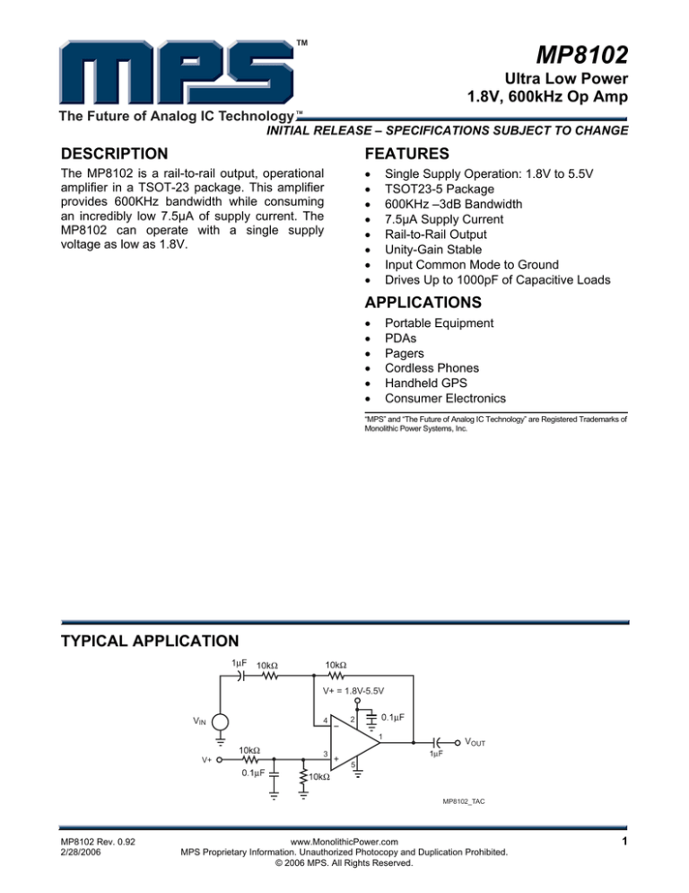
TYPICAL APPLICATION
V+ = 1.8V-5.5V
VIN
4
--
2
1
V+
3
+
VOUT
5
MP8102_TAC
MP8102 Rev. 0.92
2/28/2006
www.MonolithicPower.com
MPS Proprietary Information. Unauthorized Photocopy and Duplication Prohibited.
© 2006 MPS. All Rights Reserved.
1
TM
MP8102 – ULTRA LOW POWER, 1.8V, 600KHZ OP AMP
INITIAL RELEASE – SPECIFICATIONS SUBJECT TO CHANGE
ABSOLUTE MAXIMUM RATINGS (1)
PACKAGE REFERENCE
Supply Voltage (V+ to V-) ......................... +6.0V
Differential Input Voltage (V+ to V-).......... +6.0V
Input Voltage (VIN+ to VIN–) ..V+ + 0.3V, V– – 0.3V
TOP VIEW
OUT
1
5
V-
Recommended Operating Conditions
V+
2
IN+
3
Supply Voltage ........................... +1.8V to +5.5V
Operating Temperature .............–40°C to +85°C
4
IN-
Thermal Resistance
(3)
θJA
θJC
TSOT23-5.............................. 220 .... 110.. °C/W
MP8102_PD01_SOT23-5
Part Number*
Package
Temperature
MP8102DJ
TSOT23-5
–40°C to +85°C
*
(2)
For Tape & Reel, add suffix –Z (eg. MP8102DJ–Z)
For Lead Free, add suffix –LF (eg. MP8102DJ–LF–Z)
Notes:
1) Exceeding these ratings may damage the device.
2) The device is not guaranteed to function outside of its
operating conditions.
3) Measured on approximately 1” square of 1 oz copper.
ELECTRICAL CHARACTERISTICS
V+ = +5V, V– = 0V, VCM = V+/2, RL = 10kΩ, TA = +25°C, unless otherwise noted.
Parameter
Symbol Condition
Input Offset Voltage
Input Offset Voltage Temp
Coefficient
Input Bias Current (4)
Input Offset Current (4)
Input Voltage Range
Common-Mode Rejection
Ratio
Power Supply Rejection
Ratio
Large Signal Voltage Gain
Maximum Output Voltage
Swing
Minimum Output Voltage
Swing
Gain-Bandwidth Product
Typ
Max
Units
–5
1
+5
mV
VOS
IB
IOS
VCM
CMRR > 60dB
CMRR
0 < VCM < 3.5V
PSRR
AVOL
Supply Voltage change of
1.0V
RL = 100kΩ,
VOUT = 5.0 Peak to Peak
15
µV/°C
2
0.2
pA
pA
V
0
60
3.8
82
dB
80
dB
88
dB
VOUT
RL = 10kΩ
V+ – 23mV
V
VOUT
RL = 10kΩ
V– + 19mV
V
200
KHz
600
KHz
0.1
V/µs
20
20
7.2
mA
mA
µA
GBW
–3dB Bandwidth
BW
Slew Rate
SR
Short Circuit Current (4)
ISC
Supply Current
Min
RL = 200kΩ,CL = 2pF,
VOUT = 0
AV = 1, CL = 2pF,
RL = 1MΩ
AV = 1, CL = 2pF,
RL = 1MΩ
Source
Sink
No Load
9
Note:
4) Guaranteed by design.
MP8102 Rev. 0.92
2/28/2006
www.MonolithicPower.com
MPS Proprietary Information. Unauthorized Photocopy and Duplication Prohibited.
© 2006 MPS. All Rights Reserved.
2
TM
MP8102 – ULTRA LOW POWER, 1.8V, 600KHZ OP AMP
INITIAL RELEASE – SPECIFICATIONS SUBJECT TO CHANGE
PIN FUNCTIONS
Pin #
1
2
3
4
5
Name Description
OUT
V+
IN+
INV-
Output.
Supply Voltage.
Non-Inverting Input.
Inverting Input.
Ground or Supply Return Pin.
TEST CIRCUITS
V+
RF(+Av)
3
+
2
1
4
--
5
VOUT
U1
RFB
RF( -- Av)
S1
RL
S3
V-
S2
CL
MP8102_F01
Notes: Close S3 for positive gain. Input signal to RF(+Av) connector.
The gain Av = 1 + RFB/RIN.
For unity gain, remove RIN and short RFB.
Open S3 for negative gain. Input signal to RF(-Av) connector.
The gain Av = -RFB/RIN.
S1 and S2 are switches for possible resistor and capacitor load
connections.
Figure 1—AC Test Circuit
MP8102 Rev. 0.92
2/28/2006
www.MonolithicPower.com
MPS Proprietary Information. Unauthorized Photocopy and Duplication Prohibited.
© 2006 MPS. All Rights Reserved.
3
TM
MP8102 – ULTRA LOW POWER, 1.8V, 600KHZ OP AMP
INITIAL RELEASE – SPECIFICATIONS SUBJECT TO CHANGE
TEST CIRCUITS (continued)
+
+
+
V+
BNC
INPUT
3
+
2
1
--
OUTPUT
5
+
+
+
4
BNC
V-MP8102_F02
Figure 2—Positive Power Supply Rejection Ratio Measurement
MP8102 Rev. 0.92
2/28/2006
www.MonolithicPower.com
MPS Proprietary Information. Unauthorized Photocopy and Duplication Prohibited.
© 2006 MPS. All Rights Reserved.
4
TM
MP8102 – ULTRA LOW POWER, 1.8V, 600KHZ OP AMP
INITIAL RELEASE – SPECIFICATIONS SUBJECT TO CHANGE
TYPICAL PERFORMANCE CHARACTERISTICS
TA = +25°C, unless otherwise noted.
Output Voltage vs.
Output Current
Output Voltage vs
Output Current
Short Circuit Current vs
Supply Voltage
Sourcing
Sinking
Sourcing
4
3
2
1
0
0
6
12
18
24
4
3
2
1
0
30
20
OUTPUT CURRENT (mA)
5
OUTPUT VOLTAGE (V)
OUTPUT VOLTAGE (V)
5
0
OUTPUT CURRENT (mA)
6
12
18
24
30
16
12
8
4
0
0.5
OUTPUT CURRENT (mA)
MP8102-TPC01
0.9
1.3
1.7
2.1
2.5
SUPPLY VOLTAGE (V)
MP8102-TPC02
MP8102-TPC03
Short Circuit Current vs
Supply Voltage
Sinking
16
VOS (mV)
OUTPUT CURRENT (mA)
20
12
8
4
0
0.5
0.9
1.3
1.7
2.1
2.5
SUPPLY VOLTAGE (V)
MP8102-TPC04
MP8102 Rev. 0.92
2/28/2006
1.2
240
0.8
160
0.4
80
0
0
-0.4
-80
-0.8
-160
0
1
2
3
4
5
0
COMMON MODE VOLTAGE (V)
MP8102-TPC05
www.MonolithicPower.com
MPS Proprietary Information. Unauthorized Photocopy and Duplication Prohibited.
© 2006 MPS. All Rights Reserved.
1
2
3
4
5
SUPPLY VOLTAGE (V)
MP8102-TPC06
5
TM
MP8102 – ULTRA LOW POWER, 1.8V, 600KHZ OP AMP
INITIAL RELEASE – SPECIFICATIONS SUBJECT TO CHANGE
TYPICAL PERFORMANCE CHARACTERISTICS (continued)
TA = +25°C, unless otherwise noted.
-20
-180
-30
-40
1K
100K
1M
Phase
-10
-90
-10
-20
-180
-270
-30
-270
-360
-40
1K
-360
FREQUENCY (Hz)
10K
100K
+90
20
0
10
-90
Phase
-20
-180
-30
-270
1K
10K
100K
GAIN (dB)
GAIN (dB)
Gain
-10
-270
1K
10K
100K
1M
MP8102-TPC09
+90
20
0
10
-90
Phase
-10
-180
-20
-270
1K
1M
10K
100K
1M
+90
0
Gain
0
-90
Phase
-10
-180
-20
-270
1K
FREQUENCY (Hz)
10K
100K
1M
FREQUENCY (Hz)
MP8102-TPC11
Close-Loop Unity Gain
Frequency Response
MP8102-TPC12
PSRR vs. Frequency
V- = -2.5V, V+ = 2.5V
V+/- = +/-2.50V, Gain = 1
21
80
18
70
15
60
CL=1000pF
CL=100pF
9
6
CL=10pF
3
0
50
PSRR (dB)
GAIN (dB)
-30
FREQUENCY (Hz)
0
MP8102-TPC10
40
30
20
10
-3
0
-6
-10
-9
1K
-180
1M
Gain
FREQUENCY (Hz)
12
-20
MP8102-TPC08
PHASE (Degree)
10
0
-90
Phase
FREQUENCY (Hz)
MP8102-TPC07
0
Gain
0
GAIN (dB)
10K
0
PHASE (Degree)
-90
Phase
+90
10
Gain
0
PHASE (Degree)
GAIN (dB)
-10
0
PHASE (Degree)
Gain
0
+90
10
PHASE (Degree)
GAIN (dB)
+90
PHASE (Degree)
GAIN (dB)
10
10K
100K
1M
FREQUENCY (Hz)
100
1K
10K
100K
1M
FREQUENCY (Hz)
MP8102-TPC13
MP8102 Rev. 0.92
2/28/2006
-20
10
MP8102-TPC14
www.MonolithicPower.com
MPS Proprietary Information. Unauthorized Photocopy and Duplication Prohibited.
© 2006 MPS. All Rights Reserved.
6
TM
MP8102 – ULTRA LOW POWER, 1.8V, 600KHZ OP AMP
INITIAL RELEASE – SPECIFICATIONS SUBJECT TO CHANGE
TYPICAL PERFORMANCE CHARACTERISTICS (continued)
TA = +25°C, unless otherwise noted.
INPUT
50mV/div.
INPUT
50mV/div.
INPUT
50mV/div.
OUTPUT
50mV/div.
OUTPUT
50mV/div.
OUTPUT
50mV/div.
MP8102-TPC15
MP8102-TPC16
MP8102-TPC17
INPUT
50mV/div.
INPUT
50mV/div.
INPUT
50mV/div.
OUTPUT
50mV/div.
OUTPUT
50mV/div.
OUTPUT
50mV/div.
MP8102 -TPC18
INPUT
50mV/div.
MP8102-TPC20
INPUT
50mV/div.
OUTPUT
50mV/div.
OUTPUT
50mV/div.
MP8102-TPC21
MP8102 Rev. 0.92
2/28/2006
MP8102-TPC19
MP8102-TPC22
www.MonolithicPower.com
MPS Proprietary Information. Unauthorized Photocopy and Duplication Prohibited.
© 2006 MPS. All Rights Reserved.
7
TM
MP8102 – ULTRA LOW POWER, 1.8V, 600KHZ OP AMP
INITIAL RELEASE – SPECIFICATIONS SUBJECT TO CHANGE
TYPICAL PERFORMANCE CHARACTERISTICS (continued)
TA = +25°C, unless otherwise noted.
INPUT
1V/div.
OUTPUT
100mV/div.
OUTPUT
200mV/div.
OUTPUT
2V/div.
1ms/div.
MP8102-TPC23
MP8102-TPC24
INPUT
0.5V/div.
INPUT
1V/div.
OUTPUT
1V/div.
OUTPUT
2V/div.
INPUT
1V/div.
OUTPUT
2V/div.
1ms/div.
1ms/div.
MP8102-TPC26
MP8102 Rev. 0.92
2/28/2006
MP8102-TPC25
1ms/div.
MP8102-TPC28
www.MonolithicPower.com
MPS Proprietary Information. Unauthorized Photocopy and Duplication Prohibited.
© 2006 MPS. All Rights Reserved.
MP8102-TPC29
8
TM
MP8102 – ULTRA LOW POWER, 1.8V, 600KHZ OP AMP
INITIAL RELEASE – SPECIFICATIONS SUBJECT TO CHANGE
APPLICATION INFORMATION
performance, all bypassing capacitors should
be located as close to the op amp as possible
and all capacitors should be low ESL
(Equivalent Series Inductance) and low ESR
(Equivalent Series Resistance). Surface mount
ceramic capacitors are ideal.
Power Supply Bypassing
Regular supply bypassing techniques are
recommended. A 10µF capacitor in parallel with
a 0.1µF capacitor on both the positive and
negative supplies is ideal. For the best
PACKAGE INFORMATION
TSOT23-5
2.90 BSC
0.950
TYP
.
3
0.950
TYP
.
C
L
2.80 BSC
1.60 BSC
3
10°TYP.
(2 plcs)
+ 4°
- 0°
0°
0.25 BSC.
±0.10
Gauge Plane
C
L
0.87±0.03
1.00
Max.
0.300(Min)
0.500(Max)
(5
PLCS)
0.400
0.00-0.10
SEATING PLANE
0.127 TYP.
10° TYP.
(2 plcs)
NOTICE: The information in this document is subject to change without notice. Please contact MPS for current specifications.
Users should warrant and guarantee that third party Intellectual Property rights are not infringed upon when integrating MPS
products into any application. MPS will not assume any legal responsibility for any said applications.
MP8102 Rev. 0.92
2/28/2006
www.MonolithicPower.com
MPS Proprietary Information. Unauthorized Photocopy and Duplication Prohibited.
© 2006 MPS. All Rights Reserved.
9
