捷多邦,您值得信赖的PCB打样专家!
MP6215
3.3V/5V, Single-Channel 1.5A
Current-Limited Power Distribution Switch
The Future of Analog IC Technology
DESCRIPTION
FEATURES
The MP6215 Power Distribution Switch features
internal current limiting to prevent damage to
host devices due to faulty load conditions. The
MP6215 operates from a 3.3V or 5V nominal
input voltage and includes a 90mΩ Power
MOSFET to handle up to 1.5A continuous load
with a 2.3A typical current limit. The MP6215
has built-in protection for both over current and
increased thermal stress. For over-current
protection (OCP), the device will limit the
current by going into a constant current mode.
•
•
•
•
•
•
•
•
•
When continuous output overload condition
exceeds power dissipation of the package, the
thermal protection will shut the part off. The
device will recover once the device temperature
reduces to approx 120°C.
•
•
•
•
•
The MP6215 is available in an MSOP8 package
with exposed pad.
1.5A Continuous Current
Accurate Current Limit
2.7V to 5.5V Supply Range
140uA Quiescent Current
Thermal-Shutdown Protection
Under-Voltage Lockout
8ms FLAG Deglitch Time
No FLAG Glitch During Power Up
Reverse Current Blocking
APPLICATIONS
Notebook PC
Set-top-box
Telecom and Network Systems
PC Card Hot Swap
USB Power Distribution
“MPS” and “The Future of Analog IC Technology” are Trademarks of Monolithic
Power Systems, Inc.
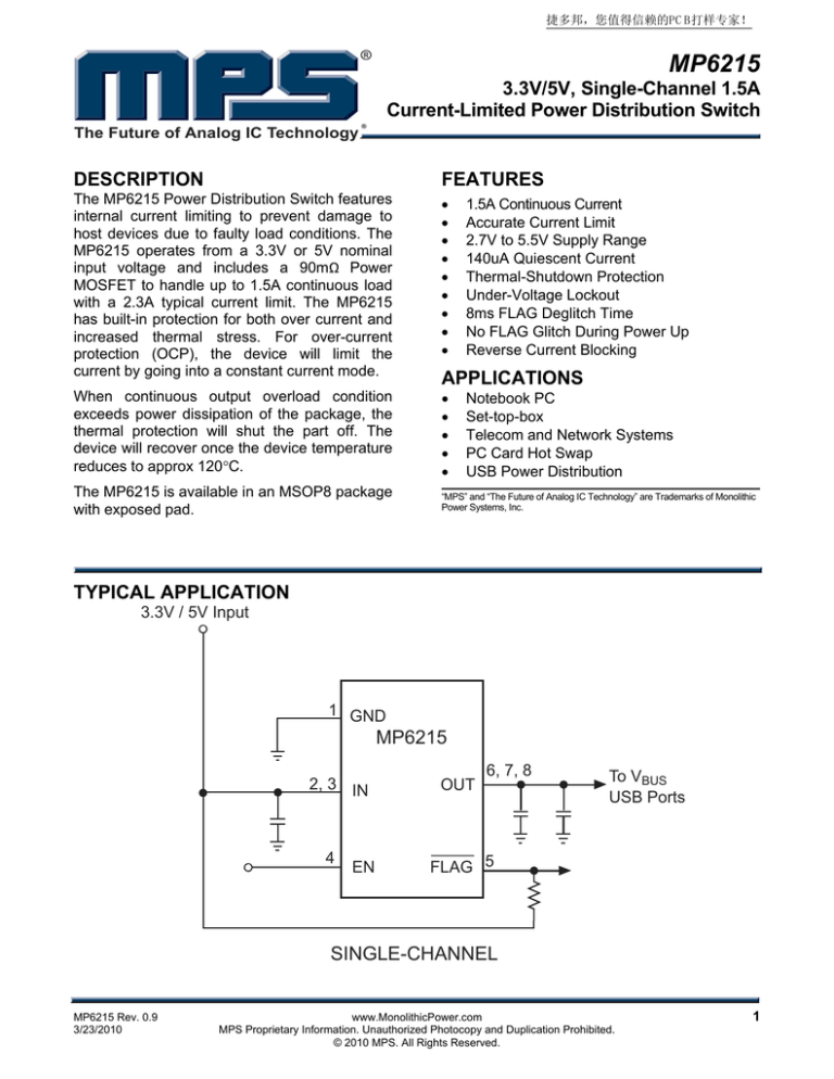
TYPICAL APPLICATION
3.3V / 5V Input
1 GND
MP6215
2, 3 IN
4
EN
OUT
6, 7, 8
To VBUS
USB Ports
FLAG 5
SINGLE-CHANNEL
MP6215 Rev. 0.9
3/23/2010
www.MonolithicPower.com
MPS Proprietary Information. Unauthorized Photocopy and Duplication Prohibited.
© 2010 MPS. All Rights Reserved.
1
MP6215 –CURRENT-LIMITED POWER DISTRIBUTION SWITCH
PACKAGE REFERENCE
TOP VIEW
GND
1
8
OUT
IN
2
7
OUT
IN
3
6
OUT
EN
4
5
FLAG
EXPOSED PAD
ON BACKSIDE
MP6215
Single-Channel
*
Part Number
Enable
Switch
Maximum
Continuous
Load Current
Typical ShortCircuit Current
@ TA=25C
MP6215DH
Active High
Single
1.5A
2.3A
Package
Temperature
MSOP8 (EP) –40°C to +85°C
For Tape & Reel, add suffix –Z (eg. MP6215DH–Z)
For RoHS Compliant Packaging, add suffix –LF
(eg. MP6215DH–LF–Z)
ABSOLUTE MAXIMUM RATINGS (1)
Thermal Resistance
IN .................................................-0.3V to +6.5V
ON, FLAG, OUT to GND..............-0.3V to +6.5V
Junction Temperature ...............................150°C
Lead Temperature ....................................260°C
Storage Temperature............... –65°C to +150°C
Operating Temperature.............. –40°C to +85°C
MSOP8E................................. 55 ...... 12... °C/W
MP6215 Rev. 0.9
3/23/2010
(2)
θJA
θJC
Notes:
1) Exceeding these ratings may damage the device.
2) Measured on JESD51-7, 4-layer PCB..
www.MonolithicPower.com
MPS Proprietary Information. Unauthorized Photocopy and Duplication Prohibited.
© 2010 MPS. All Rights Reserved.
2
MP6215 –CURRENT-LIMITED POWER DISTRIBUTION SWITCH
ELECTRICAL CHARACTERISTICS (3)
VIN=5V, TA=+25°C, unless otherwise noted.
Parameter
Condition
IN Voltage Range
Supply Current
Shutdown Current
Off Switch Leakage
Min
Typ
2.7
EN=High, IOUT=0
Device Disable, VOUT=float, VIN=5.5V
Device Disable, VIN=5.5V
Current Limit
140
1
1
1.6
Under-voltage Lockout
Under-voltage Hysteresis
FET On Resistance
EN Input Logic High Voltage
EN Input Logic Low Voltage
FLAG Output Logic Low Voltage
FLAG Output High Leakage
Current
Thermal Shutdown
Thermal Shutdown Hysteresis
VOUT Rising Time, Tr
VOUT Falling Time, Tf
Rising Edge
2.3
1.95
Max
Units
5.5
160
V
µA
µA
µA
3.0
A
2.65
0.4
0.4
V
mV
mΩ
V
V
V
1
µA
250
85
IOUT=100mA
2
ISINK=5mA
VIN=VFLAG=5.5V
140
20
°C
°C
VIN=5.5V, CL=1uF, RL=5Ω
0.9
ms
VIN=2.7V, CL=1uF, RL=5Ω
1.7
ms
VIN=5.5V, CL=1uF, RL=5Ω
0.5
ms
VIN=2.7V, CL=1uF, RL=5Ω
0.5
ms
Turn On Time, Ton
CL=100µF, RL=5Ω
3
ms
Turn Off Time, Toff
CL=100µF, RL=5Ω
10
ms
15
ms
FLAG Deglitch Time
EN Input Leakage
Reverse Leakage Current
4
-1
OUT=5.5V, IN=GND
8
0.2
µA
µA
NOTE:
3) Production test at +25°C. Specifications over the temperature range are guaranteed by design and characterization.
MP6215 Rev. 0.9
3/23/2010
www.MonolithicPower.com
MPS Proprietary Information. Unauthorized Photocopy and Duplication Prohibited.
© 2010 MPS. All Rights Reserved.
3
MP6215 –CURRENT-LIMITED POWER DISTRIBUTION SWITCH
PIN FUNCTIONS
MSOP8E
Name
Description
1
2, 3
4
GND
IN
EN
Ground.
Input Voltage. Accepts 2.7V to 5.5V input.
Active High
5
FLAG
IN-to-OUT Over-current, active-low output flag. Open-Drain.
6, 7, 8
OUT
IN-to-OUT Power-Distribution Output (for all 3 output pins)
TYPICAL PERFORMANCE CHARACTERISTICS
TA = +25ºC, unless otherwise noted.
OUTX
RL
tf
tr
CL
VO(OUTX)
90%
10%
90%
10%
TEST CIRCUIT
50%
50%
50%
VI(ENX)
50%
VI(ENX)
toff
ton
VO(OUTX)
90%
ton
VO(OUTX)
10%
toff
90%
10%
VOLTAGE WAVEFORMS
Figure 1—Test Circuit and Voltage Waveforms
MP6215 Rev. 0.9
3/23/2010
www.MonolithicPower.com
MPS Proprietary Information. Unauthorized Photocopy and Duplication Prohibited.
© 2010 MPS. All Rights Reserved.
4
MP6215 –CURRENT-LIMITED POWER DISTRIBUTION SWITCH
TYPICAL PERFORMANCE CHARACTERISTICS
TA = +25ºC, unless otherwise noted.
VEN=5V, IO=1.5A, CL=2.2uF
0.4
160
3.5
0.35
140
3
2.5
2
1.5
1
0.5
3 3.5
4 4.5
5 5.5
0.3
0.25
0.2
0.15
0.1
0.05
0
2.5
6
INPUT VOLTAGE (V)
3.5
4
4.5
5
5.5
0.4
120
0.2
110
100
0
90
5 5.5
80
2.5
6
INPUT VOLTAGE (V)
Current Limit
vs. Input Voltage
VEN=5V, CL=2.2uF
2.5
2.45
2.4
2.35
5
5.5
INPUT VOLTAGE (V)
MP6215 Rev. 0.9
3/23/2010
3 3.5
4 4.5
5 5.5
INPUT VOLTAGE (V)
6
6
6
250
Vin=5.5V
Vin=5V
200
Vin=4.5V
Vin=3.3V
150
Vin=2.7V
100
50
0
0
0.5
1
1.5
2
VEN=5V, VIN=5V, CL=2.2uF
3
2.8
2.6
2.4
3 3.5
4 4.5
5 5.5
INPUT CURRENT (V)
5 5.5
Current Limit Response Time
vs. Peak Voltage
3.2
2.2
2.5
4 4.5
OUTPUT CURRENT (A)
sCURRENT LIMIT RESPONSE
TIME (uS)
2.55
THRESHOLD TRIP CURRENT (A)
2.6
4 4.5
3 3.5
Input to Output Voltage vs.
Load Current
VEN=5V, CL=2.2uF
2.65
3.5
20
Threshold Trip Current
vs. Input Voltage
2.7
3
40
VEN=5V, CL=2.2uF
130
2.3
2.5
60
INPUT VOLTAGE (V)
140
4.5
80
VEN=5V, IOUT=1.5A, CL=2.2uF
0.6
4
100
0
2.5
6
150
3 3.5
120
Static Drain-Source
On-State Resistance vs.
Input Voltage
VEN=0V, CL=2.2uF
0.8
-0.2
2.5
VEN=5V, CL=2.2uF
INPUT VOLTAGE (V)
Supply Current, Output Disabled
vs. Input Voltage
SUPPLY CURRENT (uA)
3
INPUT TO OUTPUT VOLTAGE (mV)
0
2.5
SUPPLY CURRENT (uA)
4
TURN OFF DELAY (ms)
TURN ON DELAY (mS)
VEN=5V, IO=1.5A, CL=2.2uF
CURRENT LIMIT (A)
Supply Current, Output Enabled
vs. Input Voltage
Turn off Delay vs.
Input Votage
Turn on Delay vs.
Input Votage
6
30
25
20
15
10
5
0
3
5
7
9
11
13
PEAK CURRENT (A)
www.MonolithicPower.com
MPS Proprietary Information. Unauthorized Photocopy and Duplication Prohibited.
© 2010 MPS. All Rights Reserved.
5
MP6215 –CURRENT-LIMITED POWER DISTRIBUTION SWITCH
TYPICAL PERFORMANCE CHARACTERISTICS
TA = +25ºC, unless otherwise noted. (continued)
VOUT
2V/div
VOUT
2V/div
EN
5V/div
EN
5V/div
VOUT
2V/div
EN
5V/div
200us/div
VOUT
2V/div
VOUT
2V/div
IOUT
500mA/div
EN
5V/div
EN
5V/div
IOUT
1A/div
1ms/div
Flag
5V/div
Flag
5V/div
IOUT
500mA/div
IOUT
1A/div
1ms/div
MP6215 Rev. 0.9
3/23/2010
IOUT
1A/div
EN
5V/div
1ms/div
www.MonolithicPower.com
MPS Proprietary Information. Unauthorized Photocopy and Duplication Prohibited.
© 2010 MPS. All Rights Reserved.
2ms/div
6
MP6215 –CURRENT-LIMITED POWER DISTRIBUTION SWITCH
FUNCTION BLOCK DIAGRAM
UVLO
+
Vref
IN
Current
Sense
-- -- --
--
OUT
--
--
--
Charge
Pump
-AMP
Logic
-- FLAG
--
--
--
EN
+
Deglich
Thermat
Sense
--
--
GND
Figure2—Functional Block Diagram
DETAILED DESCRIPTION
Over Current
When the load exceeds trip current (minimum
threshold current triggering constant-current
mode) or a short is present, MP6215 switches
into to a constant-current mode (current limit
value). MP6215 will be shutdown only if the
overcurrent condition stays long enough to
trigger thermal protection.
Trigger overcurrent protection for different
overload conditions occurring in applications:
1) The output has been shorted or overloaded
before the device is enabled or input applied.
MP6215 detects the short or overload and
immediately switches into a constant-current
mode.
2) A short or an overload occurs after the device
is enabled. After the current-limit circuit has
been tripped (reached the trip current
threshold), the device switches into constantcurrent mode. However, high current may
flow for a short period of time before the
current-limit circuit can react.
MP6215 Rev. 0.9
3/23/2010
3)Output current has been gradually increased
beyond the recommended operating current.
The load current rises until the trip current
threshold is reached or until the thermal limit
of the device is exceeded. The MP6215 is
capable of delivering current up to the trip
current threshold without damaging the
device. Once the trip threshold has been
reached, the device switches into its constantcurrent mode.
Flag Response
The FLAG pin is an open drain configuration.
This FAULT will report a fail mode after an 8ms
deglitch timeout. This is used to ensure that no
false fault signals are reported. This internal
deglitch circuit eliminates the need for extend
components. The FLAG pin is not deglitched
during an over temp. or a voltage lockout.
www.MonolithicPower.com
MPS Proprietary Information. Unauthorized Photocopy and Duplication Prohibited.
© 2010 MPS. All Rights Reserved.
7
MP6215 –CURRENT-LIMITED POWER DISTRIBUTION SWITCH
Thermal Protection
The purpose of thermal protection is to prevent
damage in the IC by allowing exceptive current to
flow and heating the junction. The die
temperature is internally monitored until the
thermal limit is reached. Once this temperature is
reached, the switch will turn off and allow the
chip to cool. The switch has a built-in hysteresis.
Under-voltage Lockout (UVLO)
This circuit is used to monitor the input voltage to
ensure that the MP6215 is operating correctly.
This UVLO circuit also ensures that is no
operation until the input voltage reaches the
minimum spec.
Enable
The logic pin disables the switch to reduce
overall supply current .Once the EN pin reaches
Logic HIGH, the MP6215 is enabled.
MP6215 Rev. 0.9
3/23/2010
www.MonolithicPower.com
MPS Proprietary Information. Unauthorized Photocopy and Duplication Prohibited.
© 2010 MPS. All Rights Reserved.
8
MP6215 –CURRENT-LIMITED POWER DISTRIBUTION SWITCH
APPLICATION INFORMATION
Power-Supply Considerations
A ceramic bypass capacitor between IN and
GND, close to the device, is recommended.
Placing a high-value electrolytic capacitor on the
output pin(s) is recommended when the output
load is heavy. This precaution reduces powersupply transients that may cause ringing on the
input. Optionally, bypassing the output with a
ceramic capacitor improves the immunity of the
device to short-circuit transients.
MP6215 Rev. 0.9
3/23/2010
www.MonolithicPower.com
MPS Proprietary Information. Unauthorized Photocopy and Duplication Prohibited.
© 2010 MPS. All Rights Reserved.
9
MP6215 –CURRENT-LIMITED POWER DISTRIBUTION SWITCH
PACKAGE INFORMATION
MSOP8E (EXPOSED PAD)
0.087(2.20)
0.099(2.50)
0.114(2.90)
0.122(3.10)
5
8
0.114(2.90)
0.122(3.10)
PIN 1 ID
(NOTE 5)
0.187(4.75)
0.199(5.05)
0.062(1.58)
0.074(1.88)
Exposed Pad
0.010(0.25)
0.014(0.35)
4
1
0.0256(0.65)BSC
BOTTOM VIEW
TOP VIEW
GAUGE PLANE
0.010(0.25)
0.030(0.75)
0.037(0.95)
0.043(1.10)MAX
SEATING PLANE
0.002(0.05)
0.006(0.15)
FRONT VIEW
NOTE:
0.181(4.60)
0.040(1.00)
0.016(0.40)
0.004(0.10)
0.008(0.20)
SIDE VIEW
0.100(2.54)
0.075(1.90)
0o-6o
0.016(0.40)
0.026(0.65)
1) CONTROL DIMENSION IS IN INCHES. DIMENSION IN BRACKET IS
IN MILLIMETERS.
2) PACKAGE LENGTH DOES NOT INCLUDE MOLD FLASH,
PROTRUSION OR GATE BURR.
3) PACKAGE WIDTH DOES NOT INCLUDE INTERLEAD FLASH OR
PROTRUSION.
4) LEAD COPLANARITY (BOTTOM OF LEADS AFTER FORMING)
SHALL BE 0.004" INCHES MAX.
5) PIN 1 IDENTIFICATION HAS HALF OR FULL CIRCLE OPTION.
6) DRAWING MEETS JEDEC MO-187, VARIATION AA-T.
7) DRAWING IS NOT TO SCALE.
0.0256(0.65)BSC
RECOMMENDED LAND PATTERN
NOTICE: The information in this document is subject to change without notice. Users should warrant and guarantee that third
party Intellectual Property rights are not infringed upon when integrating MPS products into any application. MPS will not
assume any legal responsibility for any said applications.
MP6215 Rev. 0.9
3/23/2010
www.MonolithicPower.com
MPS Proprietary Information. Unauthorized Photocopy and Duplication Prohibited.
© 2010 MPS. All Rights Reserved.
10


