Three Phase DIode Bridge Rectifier
Three Phase DIode Bridge Rectifier
Project File
b ridge diode 3ph.sqproj, bridge rectifier 3ph.sqproj
Introduction
The primary objective objective of this example is to study the three phase diode-bridge rectifier circuit with the most common type of loads and filters at the output.
Simulation Example
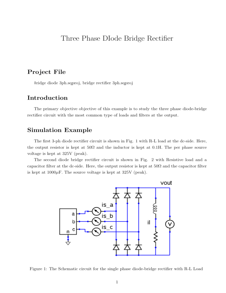
The first 3-ph diode rectifier circuit is shown in Fig. 1 with R-L load at the dc-side. Here, the output resistor is kept at 50Ω and the inductor is kept at 0 .
1H. The per phase source voltage is kept at 325V (peak).
The second diode bridge rectifier circuit is shown in Fig. 2 with Resistive load and a capacitor filter at the dc-side. Here, the output resistor is kept at 50Ω and the capacitor filter is kept at 1000 µ F. The source voltage is kept at 325V (peak).
Figure 1: The Schematic circuit for the single phase diode-bridge rectifier with R-L Load
1
Figure 2: The Schematic circuit for the single phase diode-bridge rectifier with Resistive Load and a Capacitive Filter
Sample Plots
The diode rectifier circuits are non-linear, uncontrolled rectifier circuits.
The output voltage and the source current are generally considered as the important parameters to analyze such circuits.
The simulation results of the first circuit with R-L load are shown in Fig. 3. Here, the rectified output voltage, the source current are shown along with source voltage. Due to highly inductive load the source current appears as a square wave.
The simulation results of the first circuit with Resistive load with capacitive filter are shown in Fig. 4. Here, the rectified output voltage, the source current and the individual diode currents are shown along with source voltage. Due to capacitor filter, the source current appears as narrow pulse with high peaks (spiky).
Few sample exercises are given here to get the complete understanding of the topic.
Exercises
1. Vary the output load
2. See the effect of change in output filter capacitance value.
References
[1] Ned Mohan, T.M.Undeland and W.P. Robbins, Power Electronics: Converter, Applications and Devices , Second Edition, John Wiley and Sons, 1995
2
1000
500
0
-500
20
0
10
0
-10
-20
0
18.8
18.7
18.6
18.5
18.4
18.3
18.2
0 va v_out vb is_a
0.01
is_b
0.01
il vc is_c
0.02
0.02
0.03
0.03
0.04
0.04
0.01
0.02
Time
0.03
0.04
Figure 3: Simulation Plots for a single phase diode bridge rectifier with R-L Load.
100
50
0
-50
-100
100
0
50
0
-50
-100
100
0
50
0
-50
-100
0
1000
500
0
-500
0 is_a va
0.01
0.01
0.01
vb v_out
0.01
il is_b
0.02
0.02
is_c vc
0.02
0.02
Time
0.03
0.03
0.03
0.03
0.04
0.04
0.04
0.04
Figure 4: Simulation Plots for a single phase diode bridge rectifier with Capacitive Filter.
3
