Clock Generation Whitepaper
PCI Express Refclk Jitter Compliance
1. PCI Express Overview
In the late 1990s the computing industry had taken the original parallel-data PCI bus to its practical
throughput limits. The multi-drop PCI data bus was 64 bits wide, and the clock frequency had been
pushed up to as high as 533MHz for the server-oriented variant called PCI-X. Physically, the large
number of pins required to interface to a 64-bit PCI bus had a detrimental effect on component cost. At
the system level, managing the timing skews between data lines at high clock rates was a significant
challenge.
By this time, however, the communications equipment industry had become increasingly comfortable with
gigabit per second (Gbps) serial interfaces using differential signaling. For any communication system
with 2.5Gbps or 10Gbps interfaces, the core of the system had multi-Gbps electrical signals carrying data
between cards.
In this industry context the PCI SIG (PCI Special Interest Group) adopted a revolutionary electrical layer
for its new PCI Express specification. The foundation of the PCI Express (PCIe) electrical layer is point-topoint, bidirectional, high-speed serial lanes. This foundation eliminates many of the problems associated
with the old parallel PCI bus. With the new PCIe paradigm, timing skews between wires are not an issue
because data is sent serially rather than in parallel. Also, interface pin counts are greatly reduced,
lowering component costs. In addition, system designers no longer have to be concerned with the
variable transmission distances that were present in the multi-drop PCI bus because PCIe is point-topoint not multi-drop. Also data-to-clock timing is made simple because each serial lane is self-clocked.
This is accomplished using line coding that provides a high-enough ones density to ensure that the
receiver can recover the clock along with the data.
2. Links and Speeds
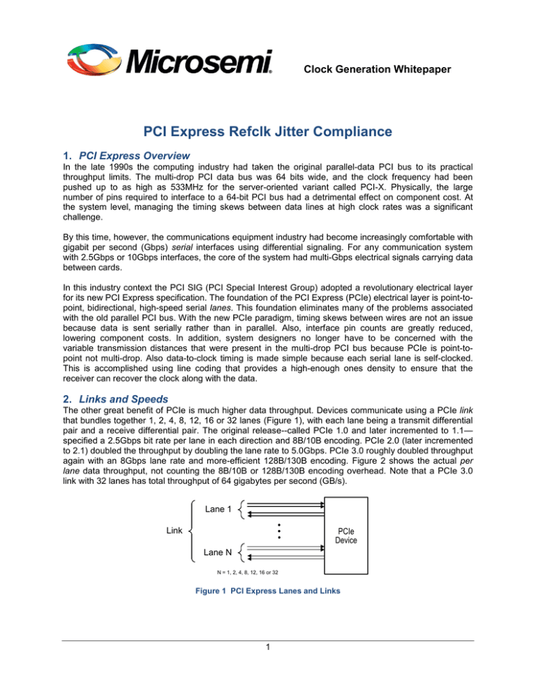
The other great benefit of PCIe is much higher data throughput. Devices communicate using a PCIe link
that bundles together 1, 2, 4, 8, 12, 16 or 32 lanes (Figure 1), with each lane being a transmit differential
pair and a receive differential pair. The original release--called PCIe 1.0 and later incremented to 1.1—
specified a 2.5Gbps bit rate per lane in each direction and 8B/10B encoding. PCIe 2.0 (later incremented
to 2.1) doubled the throughput by doubling the lane rate to 5.0Gbps. PCIe 3.0 roughly doubled throughput
again with an 8Gbps lane rate and more-efficient 128B/130B encoding. Figure 2 shows the actual per
lane data throughput, not counting the 8B/10B or 128B/130B encoding overhead. Note that a PCIe 3.0
link with 32 lanes has total throughput of 64 gigabytes per second (GB/s).
Lane 1
PCIe
Device
Link
Lane N
N = 1, 2, 4, 8, 12, 16 or 32
Figure 1 PCI Express Lanes and Links
1
PCI Express Refclk Jitter Compliance
PCIe Version
1.1
2.1
3.0
Directions
(Tx & Rx)
(b)
2
2
2
Lane Bitrate
(a)
2.5G
5.0G
8.0G
Encoding Bits
Per Byte
(c)
10
10
130÷16
Throughput Per Lane
=axb÷c
0.5GB/s
1GB/s
~2GB/s (1.969)
Figure 2 PCI Express Per-Lane Throughput
3. Refclk Signal Format
To standardize the Refclk signal used between system boards and add-in cards from multiple vendors,
the PCIe Card Electromechanical Specification Revision 2.0 specifies a differential signal format with a
common-mode voltage in the 250 to 550mV range and a differential swing (Refclk+ minus Refclk-) of at
least 150mV. This signal format is commonly called HCSL. It is considered to have a 0 to 700mV singleended swing and is source terminated.
For systems where all components are on the same card or systems where all cards are made by one
vendor, HCSL signal format is not required. Refclk can be another signal format such as LVDS, LVPECL
or CML.
4. Typical Application
Figure 3 shows a typical PCI Express application using the Common Refclk Rx architecture. A central
PCIe clock generator on the motherboard (compute application) or central processing/switching board
(telecom application) creates the original 100MHz Refclk. This clock generator can be configured for
spread-spectrum clocking to be on or off as needed by the system. The Refclk signal is then replicated by
one or more fanout buffers to provide Refclk to all other PCIe devices in the system.
Motherboard
data
clock generator
25M
xtal
±100ppm
PCIe
Device
PCIe
Device
PCIe
Device
Card 1
Card 2
ZL30251
PCIe
Device
ZL40207
Card N
Refclk
fanout buffer
Figure 3 Typical PCI Express Application
2
PCI Express Refclk Jitter Compliance
5. Refclk and Refclk Clocking Architectures
The PCIe 3.0 Base Specification, in sections 4.3.7 (for 5GT/s lanes) and 4.3.8 (for 8GT/s lanes),
describes the three Refclk architectures listed in Figure 4. It also specifies that Refclk frequency must be
100MHz ± 300ppm and that spread spectrum clocking (SSC) may be used for EMI reduction. The SSC
parameters are -0.5% down-spread with 30kHz to 33kHz modulation rate. See Microsemi’s Spread
Spectrum Whitepaper for more details about SSC.
Description
Spread
Spectrum
Modulation
Common Refclk Rx
Same 100MHz±300ppm Refclk to transmitter and receiver.
Most widely used architecture.
Yes
Data Clocked Rx
100MHz±300ppm Refclk to transmitter only.
Receiver recovers clock from incoming serial data.
More difficult jitter requirements than Common Refclk Rx.
Yes
Separate Refclk
Separate 100MHz±300ppm Refclks to Tx and Rx.
Much tighter jitter requirements.
Not as thoroughly specified as other architectures.
Not covered further in this document.
No
Architecture
Figure 4 PCI Express Refclk Architectures
The Common Refclk Rx architecture is the easiest and most commonly used method for clock distribution
among PCIe devices. Although the Data Clocked Rx architecture has a simpler block diagram, its jitter
requirements are more difficult to meet because less filtering is applied. The Common Refclk Rx
architecture has the filtering of the receiver clock multiplier PLL (Rx PLL in Figure 4-89 of PCIe 3.0), but
the Data Clocked Rx architecture does not.
Sections 4.3.7 and 4.3.8 of the PCIe 3.0 Base Specification develop models and jitter-transfer functions
for the three architectures. They also specify maximum jitter values and filters to be applied during
measurement.
3
PCI Express Refclk Jitter Compliance
6. Common Refclk Rx Architecture Jitter Requirements
Device 1
Device 2
PCIe
Link
Tx
Latch
Rx
Latch
CDR
H1(s)
low-pass
Tx
PLL
Rx
PLL
T1
H2(s)
low-pass
T2
ZL30251
Clock Generator
100MHz
±300ppm
Figure 5 Common Refclk Rx Architecture Model
In the Common Refclk Rx architecture the same reference clock is distributed to both transmit (Tx) and
receive (Rx) devices as shown in Figure 5. The jitter of concern at the receiving device is, generally
speaking, the difference between the transmit path jitter transfer function and the receive path jitter
transfer function, taking into account the delay difference between the transmit path and receive path, T =
|T1 – T2|. Each generation of PCIe has a slightly different expression of the overall transfer function, as
nd
described in the subsections below, but all generations assume 2 -order transfer functions for both Tx
and Rx PLLs. Therefore:
( )
6.1
( )
and
Common Refclk Rx Architecture, PCIe 1.1 (2.5GT/s)
The following are the Refclk transfer function aspects for PCIe 1.1:
Transfer function
H(s) = [H1(s) – H2(s)e ]H3(s)
Delay Delta, T
10ns max
H3(s)
Tx PLL Parameters, H1(s)
-3dB Freq (MHz) Max Peaking
f1
dB
22
3.0
Natural Freq (Mrad/s)
11.83*2 max
0.54
Rx PLL Parameters, H2(s)
-3dB Freq (MHz) Max Peaking
f2
dB
1.5
3.0
Natural Freq (Mrad/s)
Damping Factor
-sT
Damping Factor
1
1
2
0.807*2 max
The jitter requirements, after applying the filtering listed above, are as follows:
4
2
0.54
PCI Express Refclk Jitter Compliance
Jitter Requirement
Description
Total Jitter
Total Jitter
Conditions
12
10 Samples
6
10 Samples
Min
Max
108
86
Units
ps
ps
12
The 10 Samples requirement is the real goal but scopes do not have enough memory to test that
6
requirement directly. Therefore the 10 Samples requirement is typically tested instead.
6.2
Common Refclk Rx Architecture, PCIe 2.1 (5GT/s)
The following are the Refclk transfer function aspects for PCIe 2.1:
Transfer function
H(s) = [H1(s)e
Delay Delta, T
12ns max
H3(s)
HF (>1.5MHz):
if(f ≥ 1.5MHz) then 1 else 10
LF (10kHz-1.5MHz):
if f<10kHz then 10
elseif f<1.5MHz then 1.0
-3
else 10
– H2(s)]H3(s)
-3
-3
Tx PLL Parameters, H1(s)
-3dB Freq (MHz)
f1
5
8
-sT
Max Peaking
dB
1.0
3.0
Natural Freq (Mrad/s)
Damping Factor
1
1
1.82*2 max
4.31*2 max
1.16
0.54
Natural Freq (Mrad/s)
Damping Factor
Rx PLL Parameters, H2(s)
-3dB Freq (MHz)
f2
16
Max Peaking
dB
3.0
2
2
0.54
8.61*2 max
The two rows in the Tx PLL table represent two separate options specified in the standard. Jitter
compliance must be checked for each option in combination with the other aspects listed above.
Note that the H3(s) function is from PCIe Base Specification Revision 2.1, section 4.3.3.1 where it is
denoted as Hhi-5GT/s for the high band and Hlo-5GT/s for the low band. This function is designed to remove
spread spectrum clocking and other low-frequency jitter components that are trackable by the Rx CDR
from the high-band measurement.
The jitter requirements, after applying each of the filtering options listed above, are as follows:
Jitter Requirements
Symbol
Description
TREFCLK_HF-RMS >1.5 MHz to Nyquist jitter
TREFCLK_LF-RMS 10kHz to 1.5MHz jitter
5
Min
Max
3.1
3.0
Units
ps RMS
ps RMS
PCI Express Refclk Jitter Compliance
6.3
Common Refclk Rx Architecture, PCIe 3.0 (8GT/s)
The following are the Refclk transfer function aspects for PCIe 3.0:
Transfer functions
H(s) = [H1(s)e
-sT
H’(s) = [H2(s)e
Delay Delta, T
H3(s) (Rx CDR)
Tx PLL Parameters, H1(s)
-3dB Freq (MHz) Max Peaking
f1
dB
2.0
0.01
2.0
2.0
4.0
0.01
4.0
2.0
-sT
– H2(s)]H3(s)
– H1(s)]H3(s)
12ns max
Natural Freq (Mrad/s)
Damping Factor
1
1
0.448
6.02
0.896
12.04
14
0.73
14
0.73
Natural Freq (Mrad/s)
Damping Factor
Rx PLL Parameters, H2(s)
-3dB Freq (MHz)
f2
2.0
2.0
5.0
5.0
Max Peaking
dB
0.01
1.0
0.01
1.0
2
2
0.448
4.62
1.12
11.53
14
1.15
14
1.15
The four rows in the Tx PLL table represent four separate options specified in the standard. Similarly, four
separate Rx PLL options and two transfer functions are specified in the standard. This means that jitter
compliance must be checked for 32 options (4 x 4 x 2).
The jitter requirement, after applying each of the 32 filtering options listed above, is as follows:
Jitter Requirement
Symbol
Description
TREFCLK_RMS_CC RMS Refclk jitter for common
Refclk Rx architecture
6
Min
Max
1.0
Units
ps RMS
PCI Express Refclk Jitter Compliance
7. Data Clocked Rx Architecture Jitter Requirements
Device 1
Device 2
PCIe
Link
Tx
Latch
Rx
Latch
CDR
H1(s)
low-pass
Tx
PLL
H3(s)
low-pass
(8GT/s)
ZL30251
Clock Generator
100MHz
±300ppm
Figure 6 Data Clocked Rx Architecture Model
In the Data Clocked Rx architecture the receiver does not use Refclk directly. Instead it recovers clock
from the incoming data, which is 8B/10B or 128B/130B encoded to ensure sufficient ones density for
clock recovery. This architecture is not defined for PCIe 1.1.
nd
The Tx PLL transfer function is assumed to be 2 -order, therefore:
7.1
( )
Data Clocked Rx Architecture, PCIe 2.1 (5GT/s)
The following are the Refclk transfer function aspects for PCIe 2.1:
Transfer function
H(s) = H1(s)*H3(s)
H3(s)
HF (>1.5MHz):
if(f ≥ 1.5MHz) then 1 else 10
LF (10kHz-1.5MHz):
if f<10kHz then 10
elseif f<1.5MHz then 1.0
-3
else 10
Tx PLL Parameters, H1(s)
-3dB Freq (MHz) Max Peaking
f1
dB
16
0.5
16
3.0
-3
Natural Freq (Mrad/s)
1
8.61*2
8.61*2
-3
Damping Factor
1
1.75
0.54
The two rows in the Tx PLL table represent the minimum and maximum Tx PLL damping factor specified
in the standard. Jitter compliance must be checked for each option in combination with the other aspects
listed above.
Note that the H3(s) function is from PCIe Base Specification Revision 2.1, section 4.3.3.1 where it is
denoted as Hhi-5GT/s for the high band and Hlo-5GT/s for the low band. This function is designed to remove
low-frequency jitter components that are trackable by the Rx CDR from the high-band measurement.
The jitter requirements, after applying each of the filtering options listed above, are as follows:
7
PCI Express Refclk Jitter Compliance
Jitter Requirement
Symbol
Description
TREFCLK_HF-RMS 1.5 MHz to Nyquist jitter
TREFCLK_LF-RMS 10kHz to 1.5MHz jitter
7.2
Min
Max
4.0
7.5
Units
ps RMS
ps RMS
Data Clocked Rx Architecture, PCIe 3.0 (8GT/s)
The following are the Refclk transfer function aspects for PCIe 3.0:
Transfer function
H3(s) (Rx CDR)
Tx PLL Parameters, H1(s)
-3dB Freq (MHz)
f1
2
2
2
4
4
5
5
H(s) = H1(s)*[1-H3(s)]
Max Peaking
dB
0.01
1
2
0.01
2
0.01
1
CDR PLL Parameters, H3(s)
-3dB Freq (MHz) Max Peaking
f3
dB
10
0.5
10
2.0
Natural Freq (Mrad/s)
Damping Factor
1
1
0.448
4.62
6.02
0.896
12.04
1.12
11.53
14
1.15
0.73
14
0.73
14
1.15
Natural Freq (Mrad/s)
Damping Factor
3
3
16.57
33.8
1.75
0.73
The seven rows in the Tx PLL table represent seven separate options specified in the standard. Similarly,
two separate CDR PLL options are specified in the standard. This means that jitter compliance must be
checked for 14 options (7 x 2). (Note that PCIe appears to have eight Tx PLL cases, but it lists the 2MHz
bandwidth, 0.01dB peaking case in two places.)
The jitter requirement, after applying each of the 14 filtering options listed above, is as follows:
Jitter Requirement
Symbol
Description
TREFCLK_RMS_CC RMS Refclk jitter for data
clocked Rx architecture
Min
Max
1.0
Units
ps RMS
8. Conclusion
This document shows the complexity of verifying Refclk generator compliance with three generations of
PCI Express specifications. Overall, five PCIe clocking design options must be evaluated: Common
Refclk Rx architecture at 2.5, 5 and 8GT/s and Data Clocked architecture at 5 and 8GT/s. Each of these
options requires the application of up to 32 different filter combinations before determining actual jitter
performance. Microsemi evaluates each of its clock synthesis products for all PCIe design options and
filters to ensure that devices are fully compliant for use in PCIe clock generation applications.
8
PCI Express Refclk Jitter Compliance
9. References
PCI Express Base Specification Revision 1.1, March 28, 2005.
PCI Express Base Specification Revision 2.1, March 4, 2009.
PCI Express Base Specification Revision 3.0, November 10, 2010.
PCI Express Card Electromechanical Specification Revision 2.0, April 11, 2007.
9
PCI Express Refclk Jitter Compliance
Appendix A. Transfer Function Graphs
Common Refclk Rx Architecture
10
PCI Express Refclk Jitter Compliance
11
PCI Express Refclk Jitter Compliance
12
PCI Express Refclk Jitter Compliance
Data-Clocked Rx Architecture
13
PCI Express Refclk Jitter Compliance
14
Microsemi Corporate Headquarters
One Enterprise
Aliso Viejo, CA 92656 USA
Within the USA: +1 (800) 713-4113
Outside the USA: +1 (949) 380-6100
Sales: +1 (949) 380-6136
Fax: +1 (949) 215-4996
E-mail: sales.support@microsemi.com
©2015 Microsemi Corporation. All
rights reserved. Microsemi and the
Microsemi logo are trademarks of
Microsemi Corporation. All other
trademarks and service marks are the
property of their respective owners.
Microsemi Corporation (Nasdaq: MSCC) offers a comprehensive portfolio of semiconductor
and system solutions for communications, defense & security, aerospace and industrial
markets. Products include high-performance and radiation-hardened analog mixed-signal
integrated circuits, FPGAs, SoCs and ASICs; power management products; timing and
synchronization devices and precise time solutions, setting the world’s standard for time;
voice processing devices; RF solutions; discrete components; security technologies and
scalable anti-tamper products; Power-over-Ethernet ICs and midspans; as well as custom
design capabilities and services. Microsemi is headquartered in Aliso Viejo, Calif., and has
approximately 3,400 employees globally. Learn more at www.microsemi.com.
Microsemi makes no warranty, representation, or guarantee regarding the information contained herein
or the suitability of its products and services for any particular purpose, nor does Microsemi assume
any liability whatsoever arising out of the application or use of any product or circuit. The products sold
hereunder and any other products sold by Microsemi have been subject to limited testing and should
not be used in conjunction with mission-critical equipment or applications. Any performance
specifications are believed to be reliable but are not verified, and Buyer must conduct and complete all
performance and other testing of the products, alone and together with, or installed in, any endproducts. Buyer shall not rely on any data and performance specifications or parameters provided by
Microsemi. It is the Buyer’s responsibility to independently determine suitability of any products and to
test and verify the same. The information provided by Microsemi hereunder is provided “as is, where is”
and with all faults, and the entire risk associated with such information is entirely with the Buyer.
Microsemi does not grant, explicitly or implicitly, to any party any patent rights, licenses, or any other IP
rights, whether with regard to such information itself or anything described by such information.
Information provided in this document is proprietary to Microsemi, and Microsemi reserves the right to
make any changes to the information in this document or to any products and services at any time
without notice.
