MP18021A
100V, 2.5A, High Frequency
Half-Bridge Gate Driver
The Future of Analog IC Technology
DESCRIPTION
FEATURES
The MP18021A is a high-frequency, 100V, half
bridge, N-channel power MOSFET driver. Its low
side and high side driver channels are
independently controlled and matched with a time
delay of less than 5ns. Under-voltage lockout on
both high side and low side supplies force their
outputs low in case of insufficient supply. The
integrated bootstrap diode reduces external
component count.
Drives N-Channel MOSFET Half Bridge
100V VBST Voltage Range
On-Chip Bootstrap Diode
Typical 16ns Propagation Delay Time
Less Than 5ns Gate Drive Matching
Drives 1nf Load with 12ns/9ns Rise/Fall
Times with 12V VDD
TTL Compatible Input
Less Than 150A Quiescent Current
UVLO for Both High Side and Low Side
In SOIC8E and QFN8 (3×3mm) Packages
APPLICATIONS
Telecom Half Bridge Power Supplies
Avionics DC-DC Converters
Two-Switch Forward Converters
Active Clamp Forward Converters
All MPS parts are lead-free, halogen free, and adhere to the RoHS
directive. For MPS green status, please visit MPS website under Quality
Assurance.
“MPS” and “The Future of Analog IC Technology” are Registered
Trademarks of Monolithic Power Systems, Inc.
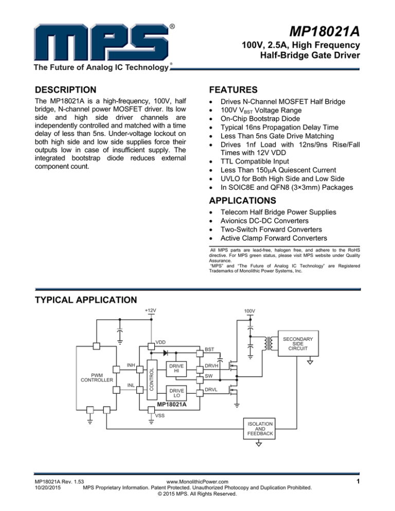
TYPICAL APPLICATION
+12V
100V
SECONDARY
SIDE
CIRCUIT
VDD
BST
PWM
CONTROLLER
INL
CONTROL
INH
DRIVE
HI
DRVH
DRIVE
LO
DRVL
SW
MP18021A
VSS
ISOLATION
AND
FEEDBACK
MP18021A Rev. 1.53
www.MonolithicPower.com
10/20/2015
MPS Proprietary Information. Patent Protected. Unauthorized Photocopy and Duplication Prohibited.
© 2015 MPS. All Rights Reserved.
1
MP18021A―100V, 2.5A, HIGH FREQUENCY HALF-BRIDGE GATE DRIVER
ORDERING INFORMATION
Part Number
Package
SOIC8E
QFN8 (3x3mm)
MP18021HN-A*
MP18021HQ-A**
Top Marking
MP18021A
ACP
* For Tape & Reel, add suffix –Z (e.g. MP18021HN–A–Z);
For RoHS compliant packaging, add suffix –LF (e.g. MP18021HN–A–LF–Z)
** For Tape & Reel, add suffix –Z (e.g. MP18021HQ–A–Z);
For RoHS compliant packaging, add suffix –LF (e.g. MP18021HQ–A–LF–Z)
PACKAGE REFERENCE
TOP VIEW
TOP VIEW
VDD
1
8
DRVL
VDD 1
8 DRVL
BST
2
7
VSS
BST 2
7 VSS
DRVH
3
6
INL
DRVH 3
6 INL
SW
4
5
INH
SW 4
5 INH
EXPOSED PAD
ON BACKSIDE
SOIC8EP
QFN8
ABSOLUTE MAXIMUM RATINGS (1)
Recommended Operating Conditions
Supply Voltage (VDD).....................-0.3V to +20V
SW Voltage (VSW) .......................-5.0V to +105V
BST Voltage (VBST) .....................-0.3V to +120V
BST to SW ....................................-0.3V to +18V
DRVH to SW ............. -0.3V to (BST-SW) + 0.3V
DRVL to VSS ...................-0.3V to (VDD + 0.3V)
All Other Pins .....................-0.3V to (VDD + 0.3V)
(2)
Continuous Power Dissipation (TA =25°C)
SOIC8E...................................................... 2.6W
QFN8 (3x3mm) .......................................... 2.5W
(2)
Continuous Power Dissipation (TA=100°C)
SOIC8E……………………………. ………0.52W
QFN8 (3x3mm)….........................…………0.5W
Junction Temperature ...............................150C
Lead Temperature ....................................260C
Storage Temperature............... -65°C to +150C
Supply Voltage (VDD) ....................... 9.0V to 18V
SW Voltage (VSW) .......................-1.0V to +100V
SW slew rate .....................................<50V/nsec
Operating Junction Temp. (TJ)..-40°C to +125°C
Thermal Resistance
(4)
θJA
(3)
θJC
SOIC8E .................................. 48 ...... 10... C/W
QFN8 (3x3mm) ....................... 50 ...... 12... C/W
Notes:
1) Exceeding these ratings may damage the device.
2) The maximum allowable power dissipation is a function of the
maximum junction temperature TJ(MAX), the junction-toambient thermal resistance θJA, and the ambient temperature
TA. The maximum allowable continuous power dissipation at
any ambient temperature is calculated by PD(MAX)=(TJ(MAX)TA)/ θJA. Exceeding the maximum allowable power dissipation
will cause excessive die temperature, and the regulator will go
into thermal shutdown. Internal thermal shutdown circuitry
protects the device from permanent damage.
3) The device is not guaranteed to function outside of its
operating conditions.
4) Measured on JESD51-7, 4-layer PCB.
MP18021A Rev. 1.53
www.MonolithicPower.com
10/20/2015
MPS Proprietary Information. Patent Protected. Unauthorized Photocopy and Duplication Prohibited.
© 2015 MPS. All Rights Reserved.
2
MP18021A―100V, 2.5A, HIGH FREQUENCY HALF-BRIDGE GATE DRIVER
ELECTRICAL CHARACTERISTICS
VDD = VBST-VSW=12V, VSS=VSW = 0V, No load at DRVH and DRVL, TA= 25C, unless otherwise noted.
Parameter
Symbol Condition
Supply Currents
VDD quiescent current
IDDQ
INL=INH=0
VDD operating current
IDDO
fsw=500kHz
Floating driver quiescent current
IBSTQ
INL=INH=0
Floating driver operating current
IBSTO
fsw=500kHz
Leakage Current
ILK
BST=SW=100V
Inputs
INL/INH High
INL/INH Low
INL/INH
internal
pull-down
RIN
resistance
Under Voltage Protection
VDD rising threshold
VDDR
VDD hysteresis
VDDH
(BST-SW) rising threshold
VBSTR
(BST-SW) hysteresis
VBSTH
Bootstrap Diode
Bootstrap diode VF @ 100uA
VF1
Bootstrap diode VF @ 100mA
VF2
Bootstrap diode dynamic R
RD
@ 100mA
Low Side Gate Driver
Low level output voltage
VOLL
IO=100mA
High level output voltage to rail
VOHL
IO=-100mA
VDRVL=0V, VDD=12V
Peak pull-up current
IOHL
VDRVL=0V, VDD=16V
VDRVL=VDD=12V
Peak pull-down current
IOLL
VDRVL=VDD=16V
Floating Gate Driver
Low level output voltage
VOLH
IO=100mA
High level output voltage to rail
VOHH IO=-100mA
VDRVH=0V, VDD=12V
Peak pull-up current
IOHH
VDRVH=0V, VDD=16V
VDRVH=VDD=12V
Peak pull-down current
IOLH
VDRVH=VDD=16V
Min
1
Typ
Max
Units
100
2.8
60
2.1
0.05
150
3.5
90
3
1
µA
mA
µA
mA
A
2
1.4
2.4
V
V
185
7.7
6.7
8.1
0.5
7.1
0.55
k
8.5
7.5
0.5
0.9
2.5
V
V
V
V
V
V
0.15
0.45
1.5
2.5
2.5
3.5
0.22
0.6
V
V
A
A
A
A
0.15
0.45
1.5
2.5
2.5
3.5
0.22
0.6
V
V
A
A
A
A
MP18021A Rev. 1.53
www.MonolithicPower.com
10/20/2015
MPS Proprietary Information. Patent Protected. Unauthorized Photocopy and Duplication Prohibited.
© 2015 MPS. All Rights Reserved.
3
MP18021A―100V, 2.5A, HIGH FREQUENCY HALF-BRIDGE GATE DRIVER
ELECTRICAL CHARACTERISTICS (continued)
VDD = VBST-VSW=12V, VSS=VSW = 0V, No load at DRVH and DRVL, TA= 25C, unless otherwise noted.
Parameter
Symbol
Switching Spec. --- Low Side Gate Driver
Turn-off propagation delay
TDLFF
INL falling to DRVL falling
Turn-on propagation delay
TDLRR
INL rising to DRVL rising
DRVL rise time
DRVL fall time
Switching Spec. --- Floating Gate Driver
Turn-off propagation delay
TDHFF
INL falling to DRVH falling
Turn-on propagation delay
TDHRR
INL rising to DRVH rising
DRVH rise time
DRVH fall time
Switching Spec. --- Matching
Floating driver turn-off to low
TMON
side drive turn-on
Low side driver turn-off to floating
TMOFF
driver turn-on
Minimum input pulse width that
TPW
changes the output
Bootstrap diode turn-on or turnTBS
off time
Over Temperature Protection(5) OTP entry threshold OTP recovery threshold OTP hysteresis Condition
Min
Typ
Max
16
Units
ns
16
CL=1nF
CL=1nF
CL=1nF
CL=1nF
12
9
ns
ns
16
ns
16
ns
12
9
ns
ns
1
5
ns
1
5
ns
50(5)
ns
10(5)
ns
160
140
20
C
Note:
5) Derived from bench characterization. Not tested in production.
INL
INPUT
(INH, INL)
INH
TDHRR, TDLRR
TDHFF, TDLFF
OUTPUT
(DRVH,
DRVL)
DRVL
TMON
TMOFF
DRVH
Figure 1—Timing Diagram
MP18021A Rev. 1.53
www.MonolithicPower.com
10/20/2015
MPS Proprietary Information. Patent Protected. Unauthorized Photocopy and Duplication Prohibited.
© 2015 MPS. All Rights Reserved.
4
MP18021A―100V, 2.5A, HIGH FREQUENCY HALF-BRIDGE GATE DRIVER
PIN FUNCTIONS
Pin #
Name
1
VDD
2
BST
3
4
5
6
7
8
Description
Supply input. This pin supplies power to all the internal circuitry. A decoupling capacitor to
ground must be placed close to this pin to ensure stable and clean supply.
Bootstrap. This is the positive power supply for the internal floating high-side MOSFET driver.
Connect a bypass capacitor between this pin and SW pin.
Floating driver output.
Switching node.
Control signal input for the floating driver.
Control signal input for the low side driver.
DRVH
SW
INH
INL
VSS,
Exposed Chip ground. Connect exposed pad to VSS for proper thermal operation.
Pad
DRVL Low side driver output.
MP18021A Rev. 1.53
www.MonolithicPower.com
10/20/2015
MPS Proprietary Information. Patent Protected. Unauthorized Photocopy and Duplication Prohibited.
© 2015 MPS. All Rights Reserved.
5
MP18021A―100V, 2.5A, HIGH FREQUENCY HALF-BRIDGE GATE DRIVER
TYPICAL PERFORMANCE CHARACTERISTICS
VDD =12V, VSS=VSW = 0V, TA= 25C, unless otherwise noted.
MP18021A Rev. 1.53
www.MonolithicPower.com
10/20/2015
MPS Proprietary Information. Patent Protected. Unauthorized Photocopy and Duplication Prohibited.
© 2015 MPS. All Rights Reserved.
6
MP18021A―100V, 2.5A, HIGH FREQUENCY HALF-BRIDGE GATE DRIVER
TYPICAL PERFORMANCE CHARACTERISTICS (continued)
VDD =12V, VSS=VSW = 0V, TA= 25C, unless otherwise noted.
MP18021A Rev. 1.53
www.MonolithicPower.com
10/20/2015
MPS Proprietary Information. Patent Protected. Unauthorized Photocopy and Duplication Prohibited.
© 2015 MPS. All Rights Reserved.
7
MP18021A―100V, 2.5A, HIGH FREQUENCY HALF-BRIDGE GATE DRIVER
BLOCK DIAGRAM
BST
VDD
UNDER
VOLTAGE
DRVH
LEVEL SHIFT
DRIVER
SW
INH
UNDER
VOLTAGE
INL
DRVL
DRIVER
VSS
Figure 2—Function Block Diagram
MP18021A Rev. 1.53
www.MonolithicPower.com
10/20/2015
MPS Proprietary Information. Patent Protected. Unauthorized Photocopy and Duplication Prohibited.
© 2015 MPS. All Rights Reserved.
8
MP18021A―100V, 2.5A, HIGH FREQUENCY HALF-BRIDGE GATE DRIVER
APPLICATION
The input signals of INH and INL can be
controlled independently. If both INH and INL are
controlling HSFET and LSFET of the same
bridge, then users must avoid shoot through by
setting sufficient dead time between INH and INL
low, and vice versa. See below figure. Dead time
is defined as the time internal between INH low
and INL low.
Shoot through
(No dead time)
Shoot through
(No dead time)
INH
INH
INL
INL
No Shoot through
No Shoot through
INH
INH
INL
INL
Dead time
Dead time
MP18021A Rev. 1.53
www.MonolithicPower.com
10/20/2015
MPS Proprietary Information. Patent Protected. Unauthorized Photocopy and Duplication Prohibited.
© 2015 MPS. All Rights Reserved.
9
MP18021A―100V, 2.5A, HIGH FREQUENCY HALF-BRIDGE GATE DRIVER
REFERENCE DESIGN CIRCUITS
Half Bridge Converter
In half-bridge converter topology, the MOSFETs
are driven alternately with some dead time.
Therefore, INH and INL are driven with
alternating signals from the PWM controller. The
input voltage can be up to 100V in this
application.
Input Voltage
Up to 100V
INH
INL
5
6
4
INH
SW
INL
DRVH 3
7
VSS
BST
8
DRVL
VDD 1
DRVL
Secondary
Circuit
2
DRVL
VDD
9V -18V
Figure 3 – Half Bridge Converter
Two-Switch Forward Converter
In two-switch forward converter topology, both
MOSFETs are turned on and off together. The
input signal (INH and INL) comes from the PWM
controller, which senses the output voltage (and
output current if current-mode control is used).
INH
INL
5
6
7
8
DRVL
INH
SW
INL
DRVH
The Schottky diodes clamp the reverse swing of
the power transformer and must be rated at the
input voltage. The input voltage can be up to
100V in this circuit.
Input Voltage
Up to 100V
4
3
2
VSS
BST
DRVL
VDD 1
VDD
Secondary
Circuit
DRVL
9V - 18V
Figure 4 – Two-Switch Forward Converter
MP18021A Rev. 1.53
www.MonolithicPower.com
10/20/2015
MPS Proprietary Information. Patent Protected. Unauthorized Photocopy and Duplication Prohibited.
© 2015 MPS. All Rights Reserved.
10
MP18021A―100V, 2.5A, HIGH FREQUENCY HALF-BRIDGE GATE DRIVER
Active-Clamp Forward Converter
In active-clamp forward converter topology, the
MOSFETs are driven alternately. The high-side
MOSFET, along with capacitor Creset, is used to
reset the power transformer in a lossless manner.
This topology lends itself well to run at duty
cycles exceeding 50%. For these reasons, the
input voltage may not be able to run at 100V for
this application.
Input Voltage
INH
INL
5
INH
SW
4
6
INL
DRVH
3
BST
2
VDD
1
7
8
DRVL
VSS
DRVL
Creset
Secondary
Circuit
DRVL
VDD
9V - 18V
Figure 5 – Active-Clamp Forward Converter
MP18021A Rev. 1.53
www.MonolithicPower.com
10/20/2015
MPS Proprietary Information. Patent Protected. Unauthorized Photocopy and Duplication Prohibited.
© 2015 MPS. All Rights Reserved.
11
MP18021A―100V, 2.5A, HIGH FREQUENCY HALF-BRIDGE GATE DRIVER
PACKAGE INFORMATION
SOIC8E
0.189(4.80)
0.197(5.00)
0.124(3.15)
0.136(3.45)
8
5
0.150(3.80)
0.157(4.00)
PIN 1 ID
1
0.228(5.80)
0.244(6.20)
0.089(2.26)
0.101(2.56)
4
TOP VIEW
BOTTOM VIEW
SEE DETAIL "A"
0.051(1.30)
0.067(1.70)
SEATING PLANE
0.000(0.00)
0.006(0.15)
0.013(0.33)
0.020(0.51)
0.0075(0.19)
0.0098(0.25)
SIDE VIEW
0.050(1.27)
BSC
FRONT VIEW
0.010(0.25)
x 45o
0.020(0.50)
GAUGE PLANE
0.010(0.25) BSC
0.050(1.27)
0.024(0.61)
0o-8o
0.016(0.41)
0.050(1.27)
0.063(1.60)
DETAIL "A"
0.103(2.62)
0.138(3.51)
RECOMMENDED LAND PATTERN
0.213(5.40)
NOTE:
1) CONTROL DIMENSION IS IN INCHES. DIMENSION IN
BRACKET IS IN MILLIMETERS.
2) PACKAGE LENGTH DOES NOT INCLUDE MOLD FLASH,
PROTRUSIONS OR GATE BURRS.
3) PACKAGE WIDTH DOES NOT INCLUDE INTERLEAD FLASH
OR PROTRUSIONS.
4) LEAD COPLANARITY (BOTTOM OF LEADS AFTER FORMING)
SHALL BE 0.004" INCHES MAX.
5) DRAWING CONFORMS TO JEDEC MS-012, VARIATION BA.
6) DRAWING IS NOT TO SCALE.
MP18021A Rev. 1.53
www.MonolithicPower.com
10/20/2015
MPS Proprietary Information. Patent Protected. Unauthorized Photocopy and Duplication Prohibited.
© 2015 MPS. All Rights Reserved.
12
MP18021A―100V, 2.5A, HIGH FREQUENCY HALF-BRIDGE GATE DRIVER
QFN8 (3×3mm)
2.90
3.10
0.30
0.50
PIN 1 ID
MARKING
0.20
0.30
2.90
3.10
PIN 1 ID
INDEX AREA
1.45
1.75
PIN 1 ID
SEE DETAIL A
8
1
2.25
2.55
0.65
BSC
4
5
TOP VIEW
BOTTOM VIEW
PIN 1 ID OPTION A
0.30x45º TYP.
PIN 1 ID OPTION B
R0.20 TYP.
0.80
1.00
0.20 REF
0.00
0.05
SIDE VIEW
DETAIL A
NOTE:
2.90
0.70
1) ALL DIMENSIONS ARE IN MILLIMETERS.
2) EXPOSED PADDLE SIZE DOES NOT INCLUDE MOLD FLASH.
3) LEAD COPLANARITY SHALL BE0.10 MILLIMETER MAX.
4) DRAWING CONFORMS TO JEDEC MO-229, VARIATION VEEC-2.
5) DRAWING IS NOT TO SCALE.
1.70
0.25
0.65
2.50
RECOMMENDED LAND PATTERN
NOTICE: The information in this document is subject to change without notice. Users should warrant and guarantee that third
party Intellectual Property rights are not infringed upon when integrating MPS products into any application. MPS will not
assume any legal responsibility for any said applications.
MP18021A Rev. 1.53
www.MonolithicPower.com
10/20/2015
MPS Proprietary Information. Patent Protected. Unauthorized Photocopy and Duplication Prohibited.
© 2015 MPS. All Rights Reserved.
13


