VOL. 11, NO. 3, FEBRUARY 2016
ISSN 1819-6608
ARPN Journal of Engineering and Applied Sciences
©2006-2016 Asian Research Publishing Network (ARPN). All rights reserved.
www.arpnjournals.com
MODELLING AND ANALYSIS OF MULTIPLE OUTPUT INVERTER
S. Sri Krishna Kumar1 and P. K. Dhal2
1
Department of Electrical and Electronics Engineering, Vel Tech High Tech Dr. RR Dr. SR Engineering College, Chennai, India
2
Department of Electrical and Electronics Engineering, Ve l Tech Dr. RR Dr. SR Technical University, Chennai, India
ABSTRACT
This paper presents an idea about multilevel inverter topology which makes use of the efficient and possible
outcomes from all the possible outputs of an inverter configuration. Low and high switching frequencies are compared, to
make use of the advantages such as reduced thermal stress and increased convertor efficiency. It is possible that the same
inverter topology can give us different levels of output voltages, provided the switching strategy is varied. The same
ideology can be used for single phase or three phase multilevel inverters. Here a single multilevel topology is taken for
consideration and the different possible output voltage levels are analysed. For simplification and ease of calculation, the
simplest configuration using two bridges is analysed.
Keywords: inverter, comparison, multilevel inverter, fundamental frequency, hybrid cascaded multilevel inverter, domestic applications.
INTRODUCTION
Multilevel inverters can be configured to produce
multiple outputs and is proved to be more suitable for high
power applications due to its lower electromagnetic
interference (EMI). Basic analysis is performed using
fundamental frequency control method. Traditionally, for
‘2n+1’ levels of output in each phase of a cascaded
multilevel inverter, ’n’ number of DC sources are required
[1-5]. But obtaining multiple DC sources for higher output
levels is very tedious. When the cascaded H-bridge
multilevel inverter is applied to a motor drive, the scheme
proposed in this paper can be used. Pulse Width
Modulation technique can be made use to trigger the
switches to conducting state. But the proposed scheme
allows us `to us a lower frequency than that of the PWM
method. Hence fundamental frequency is chosen to make
this topology useful for domestic or household
applications. Further investigations can be performed for
higher frequencies. The possibilities of all the output
levels and their performances are analysed in the
following part. For two bridges in cascade, obtaining five
level output is the basic configuration and deriving further
levels can be termed as enhanced configurations.
WORKING PRINCIPLE OF MULTI LEVEL
INVERTER TOPOLOGY
The output of a multilevel inverter yields more
than two levels of output for single phase output. This
ideology can be extended to multi-phase inverter, it says,
the multilevel inverter gives more than two levels of
output for each leg. The proper operation of a multilevel
converter is ensured by the fact that, when the number of
levels increases, the voltage blocked by switches
drastically reduces. An additional point can be given that
the multilevel inverters may be developed for any given
rating of voltage due to the fact that these inverters can be
modular in nature. There are three categories of multilevel
inverters, namely (1) Diode-clamped inverter (2)
Capacitor-clamped inverter (3) Cascade inverter. Due to
easy construction and less complexity, the multilevel
inverter configuration is made use here.
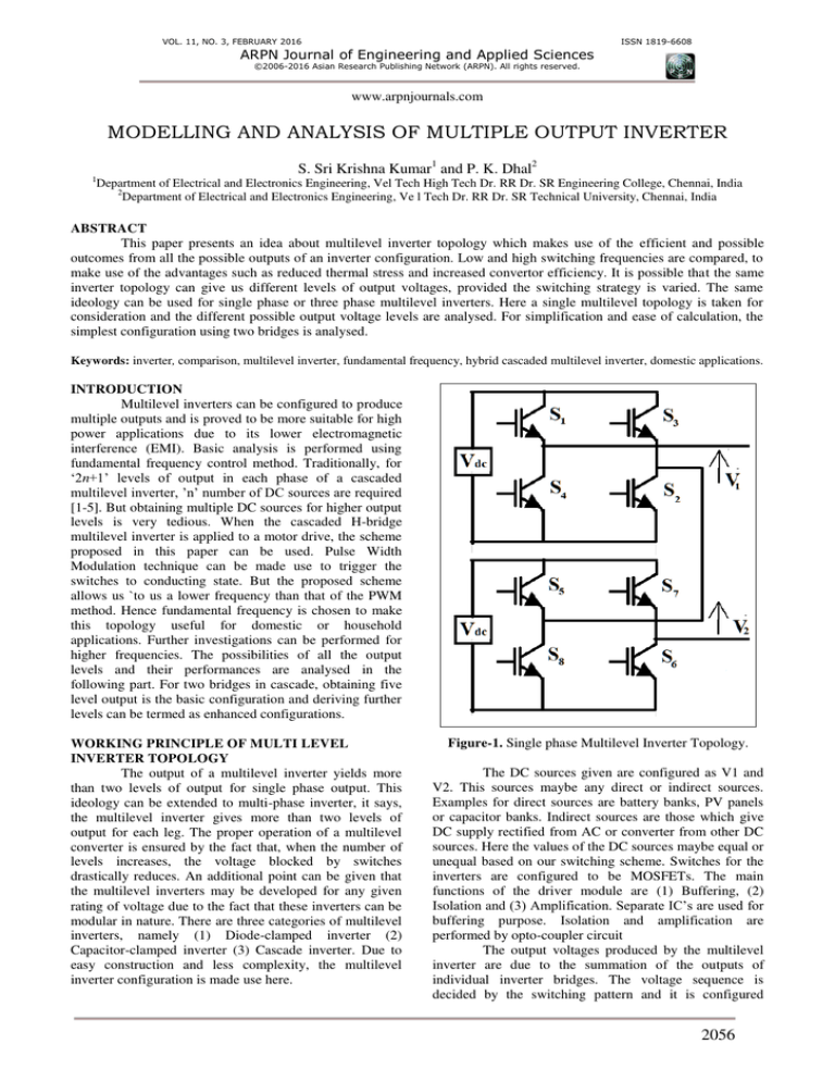
Figure-1. Single phase Multilevel Inverter Topology.
The DC sources given are configured as V1 and
V2. This sources maybe any direct or indirect sources.
Examples for direct sources are battery banks, PV panels
or capacitor banks. Indirect sources are those which give
DC supply rectified from AC or converter from other DC
sources. Here the values of the DC sources maybe equal or
unequal based on our switching scheme. Switches for the
inverters are configured to be MOSFETs. The main
functions of the driver module are (1) Buffering, (2)
Isolation and (3) Amplification. Separate IC’s are used for
buffering purpose. Isolation and amplification are
performed by opto-coupler circuit
The output voltages produced by the multilevel
inverter are due to the summation of the outputs of
individual inverter bridges. The voltage sequence is
decided by the switching pattern and it is configured
2056
VOL. 11, NO. 3, FEBRUARY 2016
ISSN 1819-6608
ARPN Journal of Engineering and Applied Sciences
©2006-2016 Asian Research Publishing Network (ARPN). All rights reserved.
www.arpnjournals.com
through the controller circuit. In general, each bridge can
produce a maximum of three levels of output. If the input
given to the inverter is V, then the output levels are +V, 0,
-V. The Separate calculations are used to determine the
phase angle of the pulses used to drive the switches. Here
the use of any discrete pulse generator circuits is replaced
by usage of a microcontroller based control circuit.
Values of V1 and V2 differ based on the inputs chosen, and
hence the output value also varies. So it can be concluded
that we can derive nine possible values of output from two
bridges in cascade. [6]
Table-1. Different voltage levels of the proposed
multilevel inverter.
H1 Output
V1
0
-V1
H2 output
Overall output
V2
V1+V2
0
V1
- V2
V1-V2
V2
V2
0
0
- V2
-V2
V2
-V1+V2
0
-V1
- V2
-V1-V2
Figure-2. Block diagram.
SWITCHING STRATEGIES FOR MULTILEVEL
INVERTER
Normally for a multilevel inverter, any of the
PWM techniques are used for switching the MOSFETs.
Any frequency can be chosen for PWM pulses.
Fundamental frequency can be used to get better results.
Also instead of complicated PWM methods, it can use a
control circuit which triggers the MOSFETs directly [5]. It
can choose 50 Hz frequency to make this topology
compatible for domestic applications.
The output voltage changes based on the phase
angle and phase delays given for a switching module. The
phase angle is calculated using the formula,
Phase angle = θ / (360*f)
Where: f= fundamental frequency
θ= angle
Phase delay = (ɸ/360)*100%
As per the topology of cascaded inverter, the
output is the summation of output voltages of individual
bridges. The bridges are termed as H1 and H2, with inputs
V1 and V2 respectively. The bridge H1 has any of the
output values as +V1, 0, -V1. Similarly the bridge H2
gives +V2, 0, -V2. For multiple output levels, various
values of inputs are chosen. To generalize the input values,
the ratio between the input values are considered.
The basic configuration with two bridges is
chosen. The voltage values given as input are assumed to
be V1 and V2. The proper switching of the bridge H1
ensures us three possible outcomes of output voltages +V 1
or 0 or –V1. Similarly the bridge H2 can possess any of the
values +V2 or 0 or –V2. When H1 gives an output V1, the
value of output given by H2 would be V2, maybe +V2 or 0
or –V2. Hence we can say, for a given output of bridge H1,
bridge H2 can deliver any of the three output values.
Table-1 given above depicts the combinational
outputs and it can be observed that the values above 0v
output are the exact negation of the values below 0v row.
In other words, we can obtain exact negative values of the
positive output voltages. And hence this configuration
gives a symmetric output. For choosing appropriate
switching cycles, the above table stands as a reference.
The output voltage values according to the given input are
given below in Table-2. Also the possible combinations
and the combinations considered for required output are
given.
All the possible values of output for the
combination of two bridges are given in Table-2. Here two
of the combinations give the same value of output in the
positive half cycle. Similarly two of the combinations give
same value of output in the negative half cycle. Hence one
from each combination can be eliminated for easy
calculations.
PROPOSED MULTIPLE OUTPUT LEVELS IN
MULTILEVEL INVERTER
For getting nine level output from two cascaded
bridges, the input voltage ratio is changed. The input
voltage ratio is maintained to be in the ratio of 3:2. Here
when the same configuration delivers a nine level output
voltage, it is symmetrical but differences between the
levels are not equal at the peak value of output. [9] But in
case of seven or five level output, the output voltage is
symmetrical and also the difference between consecutive
levels is constant.
The nine level output of the inverter topology
given above delivers a symmetric waveform. While the
inputs of the bridges are in the ratio of 3:2, the output of
the cascaded inverters would be 0, 1, ±2, 3, ±5.
Similarly, when the input voltages are equal, i.e., 1:1 ratio,
the inverter delivers a five level output. The output levels
2057
VOL. 11, NO. 3, FEBRUARY 2016
ISSN 1819-6608
ARPN Journal of Engineering and Applied Sciences
©2006-2016 Asian Research Publishing Network (ARPN). All rights reserved.
www.arpnjournals.com
would be 0, 1, ±2. For seven level output, the input
voltages considered are in the ratio 1:2. Now the output
voltages would be 0,
1, ±2,
3.
Table-2. Different voltage level combinations of the proposed multilevel inverter.
H1 Output
V1
0
-V1
H2 output
Cascaded
output
V2
V1+V2
V1+ V2
(V1=0.6V
V2=0.4V)
V
0
V1
-V2
V1+ V2
(V1=V2=V)
V1+ V2 (V1=V
V2=0.5V)
2V
1.5V
0.6V
V
V
V1-V2
0.2V
0
0.5V
V2
V2
0.4V
V
0.5V
0
0
0
0
0
-V2
-V2
-0.4V
-V
-0.5V
V2
-V1+V2
-0.2V
0
-0.5V
0
-V1
-0.6V
-V
-V
V2
-V1-V2
V
-2V
-1.5V
The operation of the proposed topology starts
with the cascaded output voltage of both the inverter
bridges being zero. Now we can represent the order of
output voltages as 0, 0.2V, 0.4V, 0.6V, V, 0.6V, 0.4V,
0.2V, 0 for positive half cycle. Considering the AC wave
to be symmetric, the negative cycle is represented as 0, 0.2V, -0.4V, -0.6V, -V, -0.6V, -0.4V, -0.2V, 0. Following
the same sequence, the order of output voltages is 0, 0.5V,
V, 1.5V, V, 0.5V, 0 and 0, -0.5V, -V, -1.5V, -V, -0.5V, 0
for positive and negative cycles of seven level output.
Comparatively, the five level output has a sequence of 0,
V, 2V, V, 0 and 0, -V, -2V, -V, 0.
As a common notation, the Ac wave is always
represented as a sinusoidal wave. This sinusoidal
representation denotes pure AC wave. But any wave that
follows the same pattern can be termed as an AC wave,
regardless of the shape. In other words, the AC wave
should start from 0V at t=0, then traverses through
variable voltage values to reach a peak value then reduce
to zero or a fixed voltage value for the entire half cycle
and the same for the negative half cycle. The positive and
negative half cycles may be symmetric or non-symmetric,
depending on the switching of the inverters.
As shown in the Table-3, the operation of the
proposed topology is designated under nine modes and
those modes are arranged in the order of maximum to
minimum value, i.e., positive cycle peak value to negative
cycle peak value.
Table-3. Different voltage level combinations of the
proposed level multilevel inverter with modes of
operation.
H1
Output
H2
output
V2
Cascaded
output
V1+V2
V1
0
V1
V2
V2
-V2
V1-V2
0
0
V2
-V1+V2
-V2
-V2
0
-V1
V2
-V1-V2
0
-V1
Mode of
operation
Figure-3. Ideal nine level output voltages.
The transition from 0V in the positive cycle
follows the modes as 5-4-3-2-1-2-3-4-5 and that for the
negative cycle is 5-6-7-8-9-8-7-6-5. Following the pattern
above, an ideal voltage waveform is given in Figure-3.
2058
VOL. 11, NO. 3, FEBRUARY 2016
ISSN 1819-6608
ARPN Journal of Engineering and Applied Sciences
©2006-2016 Asian Research Publishing Network (ARPN). All rights reserved.
www.arpnjournals.com
Table-4. Switching pattern for bridge H1.
Switches
Figure-4. Ideal seven level output voltages.
Output
S1
S2
S3
S4
0
0
0
0
0
1
1
0
0
+V1
0
0
1
1
-V1
1
1
1
1
SC
Figure-4 shows the transition for a seven level
output in the positive cycle following the modes as 4-3-21-2-3-4 and that for the negative cycle is 4-5-6-7-6-5-4.
Table-5. Switching pattern for bridge H2.
Switches
Output
S5
S6
S7
S8
0
0
0
0
0
1
1
0
0
+V2
0
0
1
1
-V2
1
1
1
1
SC
RESULTS
Figure-5. Ideal five level output voltages.
SWITCHING CYCLE OF MULTILEVEL
INVERTER
For any inverter topology to be successfully
implemented, it is mandatory that the switching pattern is
designed accurately. Since the proposed topology is
represented as a domestic purpose inverter, the frequency
is chosen to be a fundamental frequency, i.e. 50Hz.
First step is to design a switching pattern, for
which the following assumptions are made.
i.
ii.
The switches are ideal.
No two switches from the same leg conduct at any
given instant.
iii. The output voltage is exactly equal to that of the
input voltage applied for a bridge
Now the ideal output voltage wave form is taken
as the reference wave. With the assumptions made, it is
easier to find the switching angle for each switch [10].
Every individual switch is turned ON and OFF, based on
the contribution of the individual bridges to the output
voltage as represented in the ideal waveform.
Both the bridges follow the same working
principle, the only difference being the DC supply given to
each bridge. The inverter bridge H1 delivers a positive
cycle of output if switches 1 and 2 are turned ON, and
negative cycle output when switches 3 and 4 are turned
ON. Similarly for H2, positive cycle of output is obtained
if switches 5 and 6 are turned ON, and negative cycle
output when switches 7 and 8 are turned ON. The same is
explained in the following tables.
Figure-6. Output waveform for five level inverter
configuration.
Figure-7. Output waveform for seven level inverter
configuration.
2059
VOL. 11, NO. 3, FEBRUARY 2016
ISSN 1819-6608
ARPN Journal of Engineering and Applied Sciences
©2006-2016 Asian Research Publishing Network (ARPN). All rights reserved.
www.arpnjournals.com
[5] J. Laio, K. Corzine, M. Ferdowsi. 2008. A New
control method for single DC surce cascaded HBridge multilevel converters using phase-shift
modulation. IEEE Applied Power Electronics
Conference and Exposition, February. pp. 886-890.
Figure-8. Output waveform for nine level inverter
configuration.
CONCLUSIONS
The proposed topology represents a multilevel
inverter which would be efficient for domestic purposes.
The fundamental frequency, 50Hz, is taken for
consideration and a proper switching pattern is designed.
The designed switching pattern is simulated using
MATLAB software. All the ideal assumptions are taken
into account, and the proposed inverter topology is
simulated. The switches are operated with different duty
cycles for each configuration. Considering the ideal case,
the duty cycles for switches in bridge 1 and bridge 2 are
calculated. For five levels of output, switches in bridge
H1are operated at a duty of 37.5% and switches in bridge
H2 are operated at a duty of 12.5%. For seven level, all the
switches in the bridges operates at 25% and for nine level
output, all the switches are switched with a duty cycle of
31.25%. Thus it can be concluded that the switches
operates with different duty cycles for each bridge for the
basic configuration and same duty cycle for the enhanced
configuration [11].
REFERENCES
[1] J. Rodríguez, J. Lai, and F. Peng. 2002. Multilevel
inverters: a survey of topologies, controls and
applications. IEEE Transactions on Industry
Applications. vol. 49, no. 4, August, pp. 724-738
[6] L. M. Tolbert, F. Z. Peng. 1998. Multilevel converters
for large electric drives. IEEE Applied Power
Electronics Conference. pp. 530-536.
[7] Haiwen Liu, Leon M. Tolbert, Burak Ozpineci, Zhong
Du. Comparison of Fundamental Frequency and
PWM Methods Applied on a Hybrid Cascaded
Multilevel Inverter. IEEE Xplore.
[8] H. Liu, Khomfoi, L. M. Tolbert, B. Ozpineci, Z. Du.
2008. Hybridcascaded multilevel inverter with PWM
method. IEEE Power Electronics Specialists
Conference, Rhodes, Greece, June 15-19.
[9] H. Liu, L. M. Tolbert, B. Ozpineci, Z. Du. 2008.
Hybrid cascaded multilevel inverter with single DC
source. IEEE International Midwest Symposium on
Circuits and Systems, Knoxville, TN, August 10-13.
[10] S. Sirisukprasert, J. S. Lai, T. H. Liu. 2002. Optimum
harmonic reduction with a wide range of modulation
indexes for multilevel converters. IEEE Trans. Ind.
Electronics. vol. 49, no. 4, August, pp. 875-881.
[11] P. C. Loh, D. G. Holmes, T. A. Lipo. 2005.
Implementation and control of distributed PWM
cascaded multilevel inverters with minimum
harmonic distortion and common-mode voltages.
IEEE Trans. On Power Electronics, vol. 20, no. 1,
January, pp. 90-99.
[2] S. Khomfoi, L. M. Tolbert. 2007. Multilevel Power
Converters. Power Electronics Handbook, 2nd Edition
Elsevier, ISBN 978-0-12-088479-7, Chapter 17, pp.
451-482.
[3] J. Liao, K. Corzine, M. Ferdowsi. 2008. A new
control method for single-DC source cascaded HBridge multilevel converters using phase-shift
modulation. IEEE Applied Power Electronics
Conference and Exposition, February. pp. 886-890.
[4] Zhong Du, Leon M. Tolbert, Burak Ozpineci, and
John N. Chiasson. 2009. Fundamental Frequency
Switching Strategies of a Seven-Level Hybrid
Cascaded H-Bridge Multilevel Inverter. IEEE
Transactions On Power Electronics. vol. 24, no. 1,
January.
2060
