MP5120, MP5220, MP5420
High Speed, +/-9V, Rail-to-Rail Input-Output
Op Amps
The Future of Analog IC Technology
DESCRIPTION
FEATURES
The MP5120 (single), MP5220 (dual), and
MP5420 (quad) are high-speed, high-voltage
rail-to-rail input-output amplifiers for use as
voltage reference buffers in Thin Film Transistor
Liquid Crystal Displays (TFT-LCDs). The
MP5120 family provides excellent overall
performance and versatility. The 20MHz –3dB
bandwidth and 45V/µs slew rate make these
amplifier
suitable
for
many
portable
applications.
•
•
•
•
•
•
•
•
•
•
•
The MP5120, MP5220, and MP5240 are
designed to operate at supply voltages as low
as 3.2V and up to 18V at 1.6mA of supply
current per amplifier. The input can swing 0.5V
below the negative rail and 0.5V above the
positive rail. The output can swing within
100mV of each rail.
Supply Operation: +/-9V
20MHz –3dB Bandwidth
45V/µs Slew Rate
Supply Current (per amplifier)1.6mA
Unity-Gain Stable
Output Swing within 100mV of Supply Rail
Rail-to-Rail Input Capability
High Output Drive Capability (50mA)
MP5120 Available in TSOT-5
MP5220 Available in MSOP-8
MP5420 Available in TSSOP14
APPLICATIONS
•
•
•
•
•
•
•
•
•
•
•
•
The MP5420 quad channel is available in the
space-saving 14-pin TSSOP package. The
MP5220 dual channel is available in the 8-pin
MSOP package and the MP5120 single
channel is available in 5-pin TSOT package. All
feature a standard operational amplifier pin out.
TFT-LCD Drive Circuits
Electronic Notebooks
Electronic Games
Touch-Screen Displays
Personal Communication Devices
Personal Digital Assistants (PDA)
Portable Instrumentation
Sampling ADC Amplifiers
Wireless LAN
Office Automation
Active Filters
ADC/DAC Buffer
“MPS” and “The Future of Analog IC Technology” are Registered Trademarks
of Monolithic Power Systems, Inc.
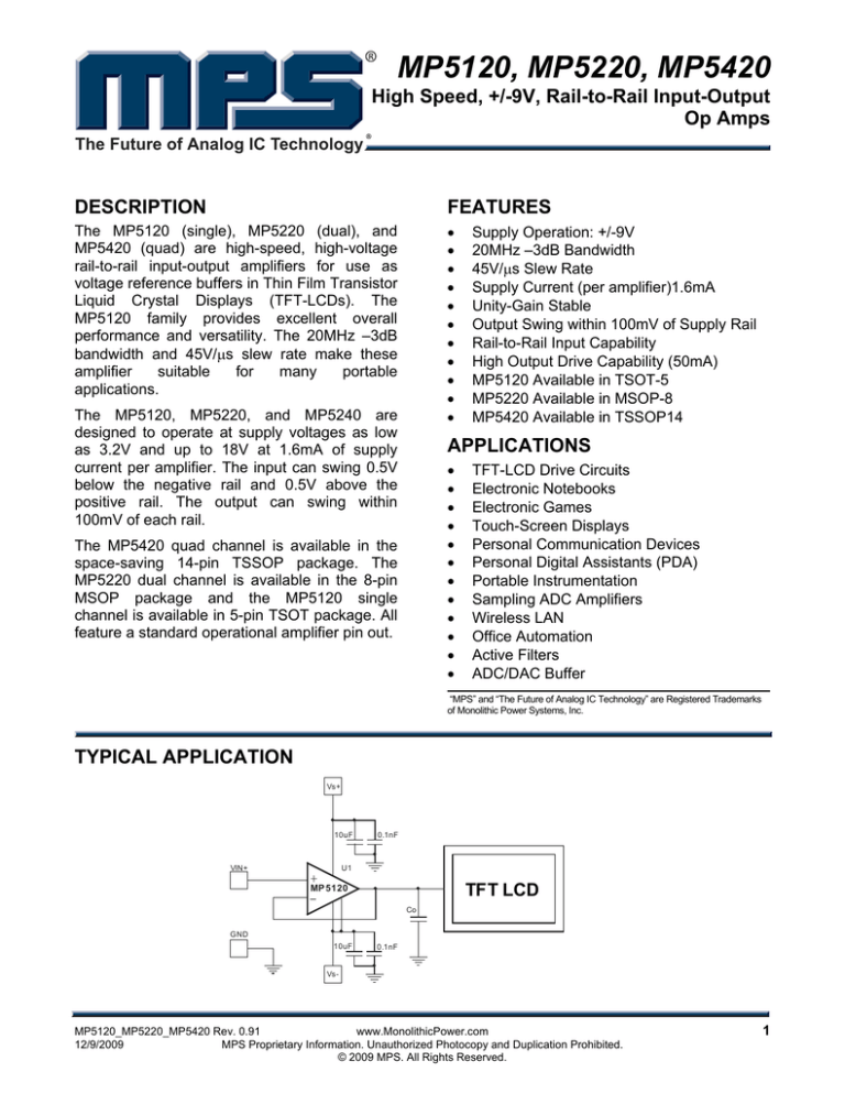
TYPICAL APPLICATION
Vs+
10uF
VIN+
0.1nF
U1
+
MP 5120
-
TFT LCD
Co
GND
10uF
0.1nF
Vs-
MP5120_MP5220_MP5420 Rev. 0.91
www.MonolithicPower.com
12/9/2009
MPS Proprietary Information. Unauthorized Photocopy and Duplication Prohibited.
© 2009 MPS. All Rights Reserved.
1
MP5120_MP5220_MP5420 –HIGH SPEED, +/-9V, RAIL-TO-RAIL INPUT-OUTPUT OP AMPS
ORDERING INFORMATION
Part Number*
MP5120DJ
MP5220DK
MP5420DM
Package
Top Marking
Free Air Temperature (TA)
TSOT
8F
–40°C to +85°C
MSOP
5220D
TSSOP
M5420DM
* For Tape & Reel, add suffix –Z (e.g. MP5120DJ–Z).
For RoHS Compliant packaging, add suffix –LF (e.g. MP5120DJ–LF–Z)
PACKAGE INFORMATION
MP5220
(8-PIN MSOP)
MP5120
(5-PIN TSOT)
TOP VIEW
TOP VIEW
VOUT 1
5 VS+
+
1
VINA-
2
--
--
VS- 2
VOUTA
8
VS+
7
VOUTB
6
VINB-
5
VINB+
+
4 VIN-
VINA+
3
VS-
4
--
VIN+ 3
+
MP5420
(14-PIN TSSOP)
TOP VIEW
14 VOUTD
VINA-
2
VINA+
3
12 VIND+
VS+
4
11
VINB+
5
10 VINC+
VINB-
6
VOUTB
7
--
+
+
--
--
+
1
+
VOUTA
13 VIND-
VS-
9 VINC8 VOUTC
--
MP5120_MP5220_MP5420 Rev. 0.91
www.MonolithicPower.com
12/9/2009
MPS Proprietary Information. Unauthorized Photocopy and Duplication Prohibited.
© 2009 MPS. All Rights Reserved.
2
MP5120_MP5220_MP5420 –HIGH SPEED, +/-9V, RAIL-TO-RAIL INPUT-OUTPUT OP AMPS
ABSOLUTE MAXIMUM RATINGS (1)
Thermal Resistance
(TA=25°C)
MSOP ....................................150 ...... 65.. °C/W
TSOT .....................................220 .... 110.. °C/W
TSSOT .....................................40 …… 6.. °C/W
Supply Voltage between VS+ and VS.....................................................–0.3V to +22V
Input Voltage......................VS- - 0.5V, VS+ +0.5V
Maximum Continuous Output Current
.................................................................. 50mA
Maximum Die Temperature ....................+125°C
Storage Temperature............... -60°C to +150°C
Ambient Operating Temp........... -40°C to +85°C
(2)
Power Dissipation. ...................... See Curves
Recommended Operating Conditions
(3)
Power Supply Operation (VS+ to VS-)
..........................................................3.2V to +18V
Operating Junct. Temp (TJ) ....... -40°C to +125°C
(4)
θJA
θJC
Notes:
1) Exceeding these ratings may damage the device.
2) The maximum allowable power dissipation is a function of the
maximum junction temperature TJ (MAX), the junction-toambient thermal resistance θJA, and the ambient temperature
TA. The maximum allowable continuous power dissipation at
any ambient temperature is calculated by PD (MAX) = (TJ
(MAX)-TA)/θJA. Exceeding the maximum allowable power
dissipation will cause excessive die temperature, and the
regulator will go into thermal shutdown. Internal thermal
shutdown circuitry protects the device from permanent
damage.
3) The device is not guaranteed to function outside of its
operating conditions.
4) Measured on JESD51-7, 4-layer PCB.
MP5120_MP5220_MP5420 Rev. 0.91
www.MonolithicPower.com
12/9/2009
MPS Proprietary Information. Unauthorized Photocopy and Duplication Prohibited.
© 2009 MPS. All Rights Reserved.
3
MP5120_MP5220_MP5420 –HIGH SPEED, +/-9V, RAIL-TO-RAIL INPUT-OUTPUT OP AMPS
ELECTRICAL CHARACTERISTICS
VS+ = +5V, VS- = -5V, RL = 10kΩ and CL = 10pF, TA =TJ= 25°C, unless otherwise noted.
Parameter
INPUT CHARACTERISTICS
Input Offset Voltage
Average
Offset
Voltage
Drift(3)
Input Bias Current
Input Impedance
Input Capacitance
Common-Mode Input Range
Common-Mode
Rejection
Ratio
Open Loop Gain
OUTPUT CHARACTERISTICS
Output Swing Low
Output Swing High
Short Circuit Current
Symbol
VOS
Settling to +0.1% (AV = +1)
-3dB Bandwidth
Gain-Bandwidth Product
Phase Margin
Channel Separation
Min
VCM=5V
IB
RIN
Typ
Max
Units
2
20
mV
5
TCVOS
VCM=5V
0.5
1
CIN
-5.5
60
85
AVOL
-4.5V ≤ VOUT ≤ +4.5V
50
60
VOL
VOH
IL = -5mA
IL = -5mA
Sourcing
Sinking
ISC
SR
tS
BW
GBWP
PM
CS
2
VS is moved from ±2.25V to
±7.75V
-4.95
4.82
70
130
70
No load
-4.0V ≤ VOUT ≤ +4.0V, 20%
to 80%
(AV = +1), VO = 2V step
RL = 10kΩ, CL = 10pF
RL = 10kΩ, CL = 10pF
RL = 10kΩ, CL = 10pF
f = 5MHz (MP5220 &
MP5420 only)
MP5120_MP5220_MP5420 Rev. 0.91
www.MonolithicPower.com
12/9/2009
MPS Proprietary Information. Unauthorized Photocopy and Duplication Prohibited.
© 2009 MPS. All Rights Reserved.
µA
GΩ
pF
+5.5
for VIN from -5.5V to +5.5V
CMRR
µ/°C
1.35
CMIR
POWER SUPPLY PERFORMANCE
Power
Supply
Rejection
PSRR
Ratio
Supply
Current
(Per
IS
Amplifier)
DYNAMIC PERFORMANCE
Slew Rate (Rise/Fall)
Condition
V
dB
≤
dB
V
V
mA
95
dB
1.6
mA
45
V/µs
500
20
14
50
ns
MHz
MHz
70
dB
4
MP5120_MP5220_MP5420 –HIGH SPEED, +/-9V, RAIL-TO-RAIL INPUT-OUTPUT OP AMPS
TYPICAL PERFORMANCE CHARACTERISTICS
VS+=5V, VS-=-5V, RL=10KΩ, CL=12pF, TA=25ºC, unless otherwise noted.
Supply Current vs.
Supply Voltage
VOS vs. VIN
1 .6
20
100
1 .4
15
90
1 .2
10
1
5
0 .8
0 .6
0
-5
0 .4
-10
0 .2
-15
2
4
6
8
-3
-2
-1
Supply Voltage (V)
40
200
50
180
40
30
160
140
Gain
120
20
100
80
Phase
Gain (dB)
Gain (dB)
60
60
40
-20
100
0
1000 10000 100000
3
10
0.1
4
200
50
150
40
50
0
-50
Phase
-100
-150
100pF
1000pF
0
0pF
-8
Magnitude (dB)
3
2
1
1000 10000 100000
Frequency (kHz)
100
50
10
0
0
Phase
-10
-50
-20
-100
-30
-150
-40
-200
-50
0.1 1 10 100 1000 10000 100000
Output Noise vs. Frequency
MP5120
10000
10k
1k
560
560
150
1000
0
100
-2
10
Av=1
-5
100
20
-1
-4
-16
10
Gain
Frequency (kHz)
-3
-12
1
150
30
Frequency Response vs. RL
4
100000
200
Frequency (kHz)
5
1000
Closed Loop Av=2
-5 0
-200
0.1 1 10 100 1000 10000 100000
12
50pF
10
Fre que ncy (kHz )
Gain
-1 0
-2 0
16
8
Gain (dB)
2
0
Frequency Response vs. CL
-4
1
20
10
Frequency ( kHz )
4
0
100
-3 0
-4 0
20
10
40
Closed Loop Av=1
80
-40
1
50
VIN ( V )
Open Loop
0
60
20
-20
-4
10 12 14 16 18
70
30
Gain (dB)
0
80
PSRR ( dB )
VOS (mV)
Supply Current (mA)
MP5120
PSRR vs. Frequency
0.1
10
1000
100000
1
0.1
Frequency (kHz)
MP5120_MP5220_MP5420 Rev. 0.91
www.MonolithicPower.com
12/9/2009
MPS Proprietary Information. Unauthorized Photocopy and Duplication Prohibited.
© 2009 MPS. All Rights Reserved.
10
1000
100000
Frequency (Hz)
5
MP5120_MP5220_MP5420 –HIGH SPEED, +/-9V, RAIL-TO-RAIL INPUT-OUTPUT OP AMPS
TYPICAL PERFORMANCE CHARACTERISTICS (continued)
VS+=5V, VS-=-5V, RL=10KΩ, CL=12pF, TA=25ºC, unless otherwise noted.
Vs+
2V/div
VIN
0.1V/div
VOUT
0.5V/div
VIN
0.1V/div
VIN
0.1V/div
VOUT
50mV/div
VOUT
0.5V/div
200ns/div
Vs+
1V/div
VIN
0.2V/div
VIN
1V/div
VOUT
1V/div
VOUT
5V/div
VOUT
1V/div
4ns/div
VIN
0.2V/div
VIN
1V/div
VOUT
1V/div
VOUT
5V/div
VOUT
2V/div
MP5120_MP5220_MP5420 Rev. 0.91
www.MonolithicPower.com
12/9/2009
MPS Proprietary Information. Unauthorized Photocopy and Duplication Prohibited.
© 2009 MPS. All Rights Reserved.
6
MP5120_MP5220_MP5420 –HIGH SPEED, +/-9V, RAIL-TO-RAIL INPUT-OUTPUT OP AMPS
OPERATION DESCRIPTION
The MP5120/MP5220/MP5420 are high-speed,
high slew rate, rail-to-rail input-output operational
amplifiers. These devices can operate up to
50mA output current and 20MHz bandwidth.
INPUT
The MP5X21 can operate with inputs from rail to
rail. It does this through the use of two differential
pairs. A traditional PNP differential pair is used
from 0.5V below the negative rail to 1V below the
positive rail. At that point the input is switched to
a NPN differential pair to operate up to 0.5V
above the positive rail. The transition from one
input differential pair to the other can cause
distortion. Inputs near the rails can also cause
distortion and degradation of other specifications.
OUTPUT
Current Rating
The MP5X21 can sink or source 50mA. It can
provide high values of peak current, and much
reduced value of average current. When the
output voltages are near the rails the ability to
provide current will be reduced.
Output Power
Make sure that the rms power is such that the die
junction temperature will remain below 125ºC.
current changes suddenly. This can damage the
part.
Transients
In addition to the ripple and noise on the power
supplies, there are also transient voltage
changes. This can be caused by another device
on the same power supply suddenly drawing
current or suddenly stopping a current draw. The
design engineer should insure that there are no
damaging transients induced on the power
supply lines when the op amp suddenly changes
current delivery.
LAYOUT
Ground Plane
Connect the opamp to a ground plane rather than
ground traces for very low impedance. If this is
not possible then make the ground traces as fat
and short as possible
Decoupling
High performance devices such as the MP5X21,
with high slew rates and high currents, need
large decoupling capacitors. These should be
placed as close to the supply pins as possible.
Use ground and power planes to make these
decoupling capacitors as effective as possible. If
that is not realistic then make the ground and
power traces as thick and short as possible.
Power Requirements
The MP5x20 family operates from a voltage
supply, of ±Vs and ground, or from a Vs split
supply. Dual supply range is ±1.6V to ±9.0V.
PSRR and Noise
A common figure of merit is the PSRR (Power
Supply Rejection Ratio). The PSRR is a measure
of how much noise gets from the supply rails into
the output. Notice that the PSRR falls with
increasing frequency. In order to have good
PSRR the ripple voltages and frequencies of the
systems switching power supplies should be
measured. If the PSRR is not acceptable,
inductors can be inserted in series with the power
supply rails to provide improved PSRR. Also
make sure there are no transients created on the
power supply lines when the MP5X21 load
MP5120_MP5220_MP5420 Rev. 0.91
www.MonolithicPower.com
12/9/2009
MPS Proprietary Information. Unauthorized Photocopy and Duplication Prohibited.
© 2009 MPS. All Rights Reserved.
7
MP5120_MP5220_MP5420 –HIGH SPEED, +/-9V, RAIL-TO-RAIL INPUT-OUTPUT OP AMPS
PACKAGE INFORMATION
TSOT23-5
0.95
BSC
0.60
TYP
2.80
3.00
5
4
1.20
TYP
1.50
1.70
1
2.60
TYP
2.60
3.00
3
TOP VIEW
RECOMMENDED LAND PATTERN
0.84
0.90
1.00 MAX
0.09
0.20
SEATING PLANE
0.30
0.50
0.95 BSC
0.00
0.10
SEE DETAIL "A"
FRONT VIEW
SIDE VIEW
NOTE:
GAUGE PLANE
0.25 BSC
0o-8o
DETAIL A
0.30
0.50
1) ALL DIMENSIONS ARE IN MILLIMETERS.
2) PACKAGE LENGTH DOES NOT INCLUDE MOLD FLASH,
PROTRUSION OR GATE BURR.
3) PACKAGE WIDTH DOES NOT INCLUDE INTERLEAD FLASH
OR PROTRUSION.
4) LEAD COPLANARITY (BOTTOM OF LEADS AFTER FORMING)
SHALL BE 0.10 MILLIMETERS MAX.
5) DRAWING CONFORMS TO JEDEC MO-193, VARIATION AA.
6) DRAWING IS NOT TO SCALE.
MP5120_MP5220_MP5420 Rev. 0.91
www.MonolithicPower.com
12/9/2009
MPS Proprietary Information. Unauthorized Photocopy and Duplication Prohibited.
© 2009 MPS. All Rights Reserved.
8
MP5120_MP5220_MP5420 –HIGH SPEED, +/-9V, RAIL-TO-RAIL INPUT-OUTPUT OP AMPS
PACKAGE INFORMATION
MSOP8
0.114(2.90)
0.122(3.10)
5
8
0.114(2.90)
0.122(3.10)
PIN 1 ID
(NOTE 5)
0.010(0.25)
0.014(0.35)
0.187(4.75)
0.199(5.05)
4
1
0.0256(0.65)BSC
BOTTOM VIEW
TOP VIEW
GAUGE PLANE
0.010(0.25)
0.030(0.75)
0.037(0.95)
0.043(1.10)MAX
SEATING PLANE
0.002(0.05)
0.006(0.15)
FRONT VIEW
0o-6o
0.016(0.40)
0.026(0.65)
0.004(0.10)
0.008(0.20)
SIDE VIEW
NOTE:
0.181(4.60)
0.040(1.00)
0.016(0.40)
1) CONTROL DIMENSION IS IN INCHES. DIMENSION IN BRACKET IS
IN MILLIMETERS.
2) PACKAGE LENGTH DOES NOT INCLUDE MOLD FLASH,
PROTRUSION OR GATE BURR.
3) PACKAGE WIDTH DOES NOT INCLUDE INTERLEAD FLASH OR
PROTRUSION.
4) LEAD COPLANARITY (BOTTOM OF LEADS AFTER FORMING)
SHALL BE 0.004" INCHES MAX.
5) PIN 1 IDENTIFICATION HAS HALF OR FULL CIRCLE OPTION.
6) DRAWING MEETS JEDEC MO-187, VARIATION AA.
7) DRAWING IS NOT TO SCALE.
0.0256(0.65)BSC
RECOMMENDED LAND PATTERN
MP5120_MP5220_MP5420 Rev. 0.91
www.MonolithicPower.com
12/9/2009
MPS Proprietary Information. Unauthorized Photocopy and Duplication Prohibited.
© 2009 MPS. All Rights Reserved.
9
MP5120_MP5220_MP5420 –HIGH SPEED, +/-9V, RAIL-TO-RAIL INPUT-OUTPUT OP AMPS
PACKAGE INFORMATION
TSSOP14
NOTICE: The information in this document is subject to change without notice. Please contact MPS for current specifications.
Users should warrant and guarantee that third party Intellectual Property rights are not infringed upon when integrating MPS
products into any application. MPS will not assume any legal responsibility for any said applications.
MP5120_MP5220_MP5420 Rev. 0.91
12/9/2009
www.MonolithicPower.com
MPS Proprietary Information. Unauthorized Photocopy and Duplication Prohibited.
© 2009 MPS. All Rights Reserved.
10


