Enpirion® Power Datasheet
ES1010SI 12V Hot-Swap Power
Distribution Controllers
DS-1044
Datasheet
The Altera® Enpirion® ES1010SI is a fully featured hot-swap
power controller that targets +12V applications. The
ES1010SI has an integrated charge pump, which can generate
a higher (6.5V) gate drive to improve efficiency.
This IC features programmable overcurrent (OC) detection,
current regulation (CR) with time delay to latch-off and softstart.
The current regulation level is set by 2 external resistors;
RISET- sets the CR Vth and the other is a low ohmic sense
resistor across, which the CR Vth is developed. The CR
duration is set by an external capacitor on the CLTIM pin,
which is charged with a 20µA current once the CR Vth level is
reached. The IC then quickly pulls down the GATE output
latching off the pass FET.
Features
• Hot-swap Single Power Distribution Control for +12V
• Overcurrent Fault Isolation
• Programmable Current Regulation Level
• Programmable Current Regulation Time to Latch-Off
• Rail-to-Rail Common Mode Input Voltage Range
• Enhanced Internal Charge Pump Drives N-Channel
MOSFET gate to 6.5V above IC bias.
• Undervoltage and Overcurrent Latch Indicators
• Adjustable Turn-On Ramp
• Protection During Turn-On
• Two Levels of Overcurrent Detection Provide Fast
Response to Varying Fault Conditions
• 1µs Response Time to Dead Short
• Pb-Free (RoHS Compliant)
Applications
• FPGA, DSP, and ASIC power protection
• Power Distribution Control
• Hot Plug Components and Circuitry
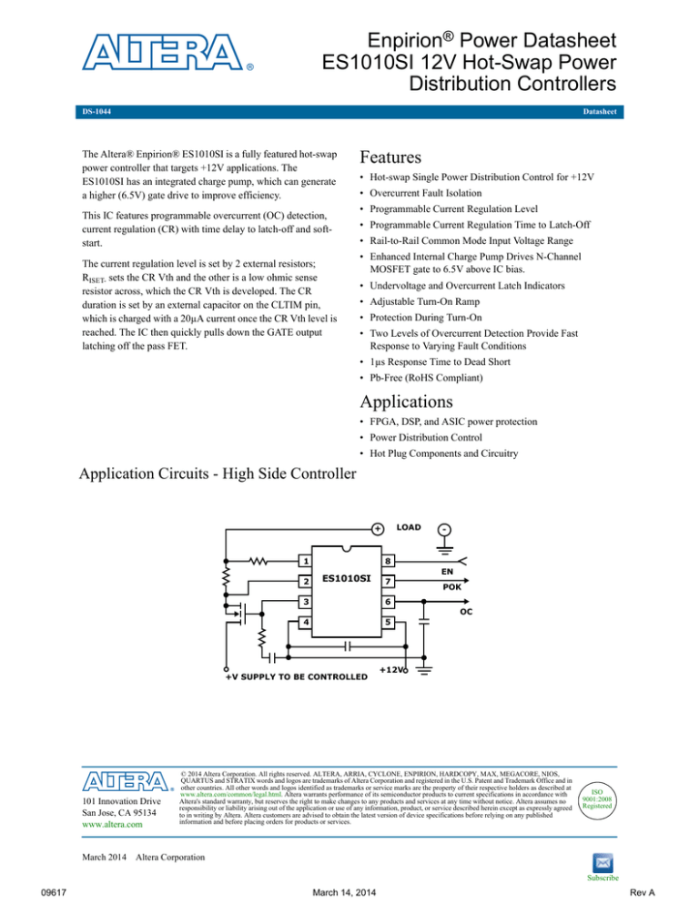
Application Circuits - High Side Controller
LOAD
+
1
2
-
8
ES1010SI
EN
7
3
6
4
5
POK
OC
+V SUPPLY TO BE CONTROLLED
101 Innovation Drive
San Jose, CA 95134
www.altera.com
March 2014
+12V
© 2014 Altera Corporation. All rights reserved. ALTERA, ARRIA, CYCLONE, ENPIRION, HARDCOPY, MAX, MEGACORE, NIOS,
QUARTUS and STRATIX words and logos are trademarks of Altera Corporation and registered in the U.S. Patent and Trademark Office and in
other countries. All other words and logos identified as trademarks or service marks are the property of their respective holders as described at
www.altera.com/common/legal.html. Altera warrants performance of its semiconductor products to current specifications in accordance with
Altera's standard warranty, but reserves the right to make changes to any products and services at any time without notice. Altera assumes no
responsibility or liability arising out of the application or use of any information, product, or service described herein except as expressly agreed
to in writing by Altera. Altera customers are advised to obtain the latest version of device specifications before relying on any published
information and before placing orders for products or services.
ISO
9001:2008
Registered
Altera Corporation
Subscribe
09617
March 14, 2014
Rev A
Page 2
Ordering Information
PART NUMBER
(Notes 1, 3)
PART
MARKING
ES1010SI
1010
EVB-ES1010SI
Evaluation Platform
TEMPERATURE
RANGE (°C)
PACKAGE
(Pb-free)
-40 to +85
8 Ld SOIC
PKG.
DWG. #
M8.15
NOTES:
1. These Altera Enpirion Pb-free plastic packaged products employ special Pb-free material sets, molding compounds/die attach materials, and
100% matte tin plate plus anneal (e3 termination finish, which is RoHS compliant and compatible with both SnPb and Pb-free soldering
operations). Altera Enpirion Pb-free products are MSL classified at Pb-free peak reflow temperatures that meet or exceed the Pb-free
requirements of IPC/JEDEC J STD-020..
Pin Configuration
ES1010SI
(8 LD SOIC)
TOP VIEW
ISET-
1
8
EN
ISEN+
2
7
POK
GATE
3
6
CLTIM
GND
4
5
VIN
Pin Descriptions
PIN
NO.
SYMBOL
1
ISET-
Current Set
Connect to the low side of the current sense resistor through the current limiting set resistor. This
pin functions as the current limit programming pin.
2
ISEN+
Current Sense
Connect to the more positive end of sense resistor to measure the voltage drop across this resistor.
3
GATE
External FET Gate Drive
Pin
Connect to the gate of the external N-Channel MOSFET. A capacitor from this node to ground
sets the turn-on ramp. At turn-on this capacitor will be charged to VIN +6.5V by an 14µA
current source.
4
GND
Chip Return
5
VIN
Chip Supply
12V chip supply. This can be either connected directly to the +12V rail supplying the switched
load voltage or to a dedicated GND +12V supply.
6
CLTIM
Current Limit Timing
Capacitor
Connect a capacitor from this pin to ground. This capacitor determines the time delay between
an overcurrent event and chip output shutdown (current limit time-out). The duration of
current limit time-out is equal to 93k x CLTIM.
7
POK
Power Good Indicator
Indicates that the voltage on the ISEN+ pin is satisfactory. POK is driven by an open drain
N-Channel MOSFET and is pulled low when the output voltage (VISEN+) is less than the UV
level for the particular IC.
8
EN
Power-ON
EN is used to control and reset the chip. The chip is enabled when EN pin is driven high to a
maximum of 5V or is left open. Do not drive this input >5V. After a current limit time-out, the
chip is reset by a low level signal applied to this pin. This input has 20µA pull-up capability.
FUNCTION
DESCRIPTION
ES1010SI 12V Hot-Swap Power Distribution Controllers
09617
March 2014
March 14, 2014
Altera Corporation
Rev A
Page 3
Absolute Maximum Ratings
Thermal Information
TA = +25°C
VIN . . . . . . . . . . . . . . . . . . . . . . . . . . . . . . . . . . . . . . . -0.3V to +16V
GATE . . . . . . . . . . . . . . . . . . . . . . . . . . . . . . . . . . .-0.3V to VIN + 8V
ISEN+, POK, EN, CLTIM, ISET- . . . . . . . . . . . -0.3V to VIN + 0.3V
Operating Conditions
JA (°C/W)
Thermal Resistance (Typical, Note 2)
8 Ld SOIC Package . . . . . . . . . . . . . . . . . . . . . .
98
Maximum Junction Temperature (Plastic Package) . . . . . . . +150°C
Maximum Storage Temperature Range . . . . . . . . . . -65°C to +150°C
Pb-Free Reflow Profile . . . . . . . . . . . . . . . . . . . . . . . . . . . . . . . . . —
VIN Supply Voltage Range . . . . . . . . . . . . . . . . . . . . . . +12V ±15%
Temperature Range (TA) . . . . . . . . . . . . . . . . . . . . . . -40°C to +85°C
ESD
Human Body Model . . . . . . . . . . . . . . . . . . . . . . . . . . . . . . . 2.5kV
Machine Model. . . . . . . . . . . . . . . . . . . . . . . . . . . . . . . . . . . .250V
CAUTION: Do not operate at or near the maximum ratings listed for extended periods of time. Exposure to such conditions may adversely impact
product reliability and result in failures not covered by warranty.
NOTES:
2. JA is measured with the component mounted on a high effective thermal conductivity test board in free air.
3. All voltages are relative to GND, unless otherwise specified.
Electrical Specifications
VIN = 12V, TA = TJ = full temperature range, Unless Otherwise Specified.
PARAMETER
SYMBOL
TEST CONDITIONS
MIN
(Note 4)
TYP
MAX
(Note 4)
UNITS
17
20
22
µA
CURRENT CONTROL
ISET- Current Source
IISET_ft
ISET- Current Source
IISET_pt
TJ = +15°C to +55°C
19
20
21
µA
Current Limit Amp Offset
Voltage
Vio_ft
VISET- - VISEN+
-4.5
0
4.5
mV
Current Limit Amp Offset
Voltage
Vio_pt
VISET- - VISEN+, TJ = +15°C to +55°C
-2
0
2
mV
GATE DRIVE
GATE Response Time to
Severe OC
pd_woc_amp
VGATE to 10.8V
-
100
-
ns
GATE Response Time to
Overcurrent
pd_oc_amp
VGATE to 10.8V
-
600
-
ns
GATE Turn-On Current
IGATE
VGATE to = 6V
10.8
14
16.7
µA
45
82
124
mA
-
0.8
-
A
8.9
9.6
10.2
V
VIN + 5.7V
VIN +
6.5V
-
V
-
3
3.9
mA
GATE Pull-Down Current
OC_GATE_I_4V
GATE Pull-Down Current
(Note 4)
WOC_GATE_I_4V
Undervoltage Threshold
12VUV_VTH
GATE High Voltage
12VG
Overcurrent
Severe Overcurrent
GATE Voltage
BIAS
VIN Supply Current
VIN POR Rising
Threshold
VIN_POR_L2H
VIN Low to High
7
8.4
9
V
VIN POR Falling
Threshold
VIN_POR_H2L
VIN High to Low
6.9
8.1
8.7
V
VIN POR Threshold
Hysteresis
VIN_POR_HYS
VIN_POR_L2H - VIN_POR_H2L
0.1
0.3
0.5
V
Maximum EN Pull-Up
Voltage
PWRN_PUV
Maximum External Pull-up Voltage
-
5
-
V
March 2014
09617
IVIN
Altera Corporation
ES1010SI 12V Hot-Swap Power Distribution Controllers
March 14, 2014
Rev A
Page 4
Electrical Specifications
PARAMETER
VIN = 12V, TA = TJ = full temperature range, Unless Otherwise Specified.
SYMBOL
TEST CONDITIONS
TYP
MAX
(Note 4)
UNITS
2.5
3.2
-
V
EN Pull-Up Voltage
VEN
EN Rising Threshold
VEN_THR
1.1
1.7
2.35
V
EN Hysteresis
EN_HYS
125
170
250
mV
IEN
12.6
17
24
µA
17.2
20.5
25
µA
-
20
-
mA
1.6
1.8
2.1
V
-
8
-
mA
EN Pull-Up Current
EN Pin Open
MIN
(Note 4)
CURRENT REGULATION DURATION/POWER GOOD
CCLTIM Charging Current
CCLTIM_ichg0
VCLTIM = 0V
CCLTIM Fault Pull-Up
Current (Note 4)
Current Limit Time-Out
Threshold Voltage
CCLTIM_Vth
Power Good Pull Down
Current
PG_Ipd
CLTIM Voltage
VOUT = 0.5V
NOTES:
4. Parameters with MIN and/or MAX limits are 100% tested at +25°C, unless otherwise specified. Temperature limits established by
characterization and are not production tested.
Simplified Block Diagram
VIN
+
POR
+
QN
8V
ISET-
+
Q
UV
R
R
EN
S
+
-
VREF
ENABLE
12V
ISEN+
POK
20µA
UV DISABLE
CLIM
OC
GATE
FALLING
EDGE
DELAY
10µA
+
-
7.5k
ENABLE
GND
+
1.86V
WOCLIM
18V
CLTIM
+
-
+
-
20µA
18V
RISING
EDGE
PULSE
VIN
Description and Operation
The ES1010SI is targeted for +12V single power supply distribution control for generic hot swap switching applications.
This ICs features a highly accurate programmable current regulation (CR) level with programmable time delay to latch-off, and
programmable soft-start turn-on ramp all set with a minimum of external passive components. It also includes severe OC protection
ES1010SI 12V Hot-Swap Power Distribution Controllers
09617
March 2014
March 14, 2014
Altera Corporation
Rev A
Page 5
that immediately shuts down the MOSFET switch should a rapid load current transient such as with a dead short cause the CR Vth to
exceed the programmed level by 150mV. Additionally, it has an UV indicator and an OC latch indicator. The functionality of the POK
feature is enabled once the IC is biased, monitoring and reporting any UV condition on the ISEN+ pin.
Upon initial power-up, the IC can either isolate the voltage supply from the load by holding the external N-Channel MOSFET
switch off or apply the supply rail voltage directly to the load for true hot swap capability. The EN pin must be pulled low for the
device to isolate the power supply from the load by holding the external N-Channel MOSFET off. With the EN pin held high or
floating the IC will be in true hot swap mode. In both cases the IC turns on in a soft-start mode protecting the supply rail from
sudden inrush current.
At turn-on, the external gate capacitor of the N-Channel MOSFET is charged with a 11µA current source resulting in a
programmable ramp (soft-start turn-on). The internal ES1010SI charge pump supplies the gate drive for the 12V supply switch
driving that gate to ~VIN +6.5V. Load current passes through the external current sense resistor. When the voltage across the sense
resistor exceeds the user programmed CR voltage threshold value, (see Table 1 for RISET- programming resistor value and resulting
nominal current regulation threshold voltage, VCR) the controller enters its current regulation mode. At this time, the time-out
capacitor, on CLTIM pin is charged with a 20µA current source and the controller enters the current limit time to latch-off period. The
length of the current limit time to latch-off duration is set by the value of a single external capacitor (see Table 2) for CCLTIM capacitor
value and resulting nominal current limited time-out to latch-off duration placed from the CLTIM pin (pin 6) to ground. The
programmed current level is held until either the OC event passes or the time-out period expires. If the former is the case then the NChannel MOSFET is fully enhanced and the CCLTIM capacitor is discharged. Once CCLTIM charges to ~1.8V signaling that the time-out
period has expired, an internal latch is set whereby the FET gate is quickly pulled to 0V turning off the N-Channel MOSFET switch,
isolating the faulty load.
TABLE 1. RISET- PROGRAMMING RESISTOR VALUE
RISET- RESISTOR
NOMINAL CR VTH
10k
200mV
4.99k
100mV
2.5k
50mV
1.25k
25mV
NOTE: Nominal Vth = RISET- x 20µA.
TABLE 2. CCLTIM CAPACITOR VALUE
CCLTIM CAPACITOR NOMINAL CURRENT LIMITED PERIOD
0.022µF
2ms
0.047µF
4.4ms
0.1µF
9.3ms
NOTE: Nominal time-out period = CCLTIM x 93k.
This IC responds to a severe overcurrent load (defined as a voltage across the sense resistor >150mV over the OC Vth set point) by
immediately driving the N-Channel MOSFET gate to 0V in about 10µs. The gate voltage is then slowly ramped up turning on the
N-Channel MOSFET to the programmed current regulation level; this is the start of the time-out period.
Upon a UV condition, the POK signal will pull low when connected through a resistor to the logic or VIN supply. This pin is a UV
fault indicator. For an OC latch-off indication, monitor CLTIM, pin 6. This pin will rise rapidly from 1.8V to VIN once the timeout period expires.
See Figures 2 through 13 for graphs and waveforms related to text.
The IC is reset after an OC latch-off condition by a low level on the EN pin and is turned on by the EN pin being driven high.
Application Considerations
Design applications where the CR Vth is set extremely low (25mV or less), there is a two-fold risk to consider.
• There is the susceptibility to noise influencing the absolute CR Vth value. This can be addressed with a 100pF capacitor across the
RSENSE resistor.
• Due to common mode limitations of the overcurrent comparator, the voltage on the ISET- pin must be 20mV above the IC
ground either initially (from ISET-*RSET) or before CCLTIM reaches time-out (from gate charge-up). If this does not happen, the IC
may incorrectly report overcurrent fault at start-up when there is no fault. Circuits with high load capacitance and initially low
load current are susceptible to this type of unexpected behavior.
Do not signal nor pull-up the EN input to > 5V. Exceeding 6V on this pin will cause the internal charge pump to malfunction.
March 2014
09617
Altera Corporation
ES1010SI 12V Hot-Swap Power Distribution Controllers
March 14, 2014
Rev A
Page 6
During the soft-start and the time-out delay duration with the IC in its current limit mode, the VGS of the external N-Channel
MOSFET is reduced driving the MOSFET switch into a (linear region) high rDS(ON) state. Strike a balance between the CR limit and
the timing requirements to avoid periods when the external N-Channel MOSFETs may be damaged or destroyed due to excessive
internal power dissipation. Refer to the MOSFET SOA information in the manufacturer’s data sheet.
When driving particularly large capacitive loads a longer soft-start time to prevent current regulation upon charging and a short CR
time may offer the best application solution relative to reliability and FET MTF.
Physical layout of RSENSE resistor is critical to avoid the possibility of false overcurrent occurrences. Ideally, trace routing
between the RSENSE resistors and the IC is as direct and as short as possible with zero current in the sense lines (see Figure 1).
CORRECT
INCORRECT
TO ISEN+ AND
RISET
CURRENT
SENSE RESISTOR
FIGURE 1. SENSE RESISTOR PCB LAYOUT
.
ES1010SI 12V Hot-Swap Power Distribution Controllers
09617
March 2014
March 14, 2014
Altera Corporation
Rev A
Page 7
Typical Performance Curves
3.5
22.0
3.4
21.5
21.0
ISET- (µA)
IDD (mA)
3.3
3.2
3.1
3.0
20.0
19.5
19.0
2.9
2.8
20.5
18.5
-40
0
25
70
TEMPERATURE (°C)
85
18.0
125
-40
85
125
1.82
20.8
20.6
20.4
1.81
CLTIM - 0V
CCLTIM VTH (V)
20.2
20.0
19.8
19.6
19.4
1.80
1.79
1.78
19.2
19.0
18.8
-40
0
25
70
85
1.77
125
-40
0
GATE TURN-ON CURRENT (µA)
9.80
9.75
9.70
9.65
9.60
-40
0
25
70
85
85
125
125
16.0
15.5
15.0
14.5
14.0
13.5
13.0
12.5
12.0
-40
0
25
70
85
125
TEMPERATURE (°C)
TEMPERATURE (°C)
FIGURE 7. GATE CHARGE CURRENT
FIGURE 6. UV THRESHOLD
March 2014
25
70
TEMPERATURE (°C)
FIGURE 5. CCLTIM OC VOLTAGE THRESHOLD
FIGURE 4. CCLTIM CURRENT SOURCE
UVTH (V)
70
FIGURE 3. ISET- SOURCE CURRENT
TEMPERATURE (°C)
09617
25
TEMPERATURE (°C)
FIGURE 2. VIN BIAS CURRENT
CLTIM CHARGE CURRENT (µA)
0
Altera Corporation
ES1010SI 12V Hot-Swap Power Distribution Controllers
March 14, 2014
Rev A
Page 8
(EQ. 1)
72 – 12
I DD1 = -----------------------1.58k
I DD1 = 38mA TypicalValue = 12Vrating, 50mA reverse current
(Continued)
8.3
22
8.2
21
VIN LO TO HI
8.1
8.0
7.9
7.8
7.7
VIN HI TO LO
7.6
7.5
-40
0
GATE VOLTAGE (V)
POWER ON RESET (V)
Typical Performance Curves
+85°C
20
+25°C
19
18
-40°C
17
16
15
14
25
70
TEMPERATURE (°C)
85
125
FIGURE 8. POWER-ON RESET VOLTAGE THRESHOLD
13
9
10
11
12
13
BIAS VOLTAGE (V)
14
15
FIGURE 9. GATE VOLTAGE vs BIAS and TEMPERATURE
EN
EN
GATE
GATE
VOUT
POK
POK
VOUT
VOUT
FIGURE 11. ES1010SI TURN-OFF
FIGURE 10. ES1010SI TURN-ON
ES1010SI 12V Hot-Swap Power Distribution Controllers
09617
March 2014
March 14, 2014
Altera Corporation
Rev A
Page 9
Typical Performance Curves
(Continued)
ILOAD
ILOAD
GATE
GATE
VOUT
VOUT
CLTIM
CLTIM
FIGURE 12. IOC REGULATION and TURN-OFF
FIGURE 13. WOC TURN-OFF and RESTART
EVB-ES1010SI Board
The EVB-ES1010SI is default provided as a +12V high side switch controller with the CR level set at ~2.5A. See Figure 11 for
EVB-ES1010SI schematic and Table 3 for BOM. Bias and load connection points are provided along with test points for each IC
pin.
With J1 installed the ES1010SI will be biased from the +12V supply (VIN) being switched. Connect the load to VLOAD+. EN pin
pulls high internally enabling the ES1010SI if not driven low via EN test point or J2.
With R3 = 1.24k the CR Vth is set to 24.8mV and with the 10m sense resistor (R1) the EVB-ES1010SI has a nominal CR level
of 2.5~A. The 0.01µF delay time to latch-off capacitor results in a nominal 1ms before latch-off of output after an OC event.
Reconfiguring the EVB-ES1010SI board for a higher CR level can be done by changing the RSENSE and/or RISET- resistor values as
the provided FET is rated for a much higher current.
AGND
VLOAD+
VOUT
R3
J2
8
1
R1
2
ES1010SI
7
3
U1
6
4
Q1
EN
POK
CCLTIM
5
C3
R2
R4
C2
C1
J1
VIN
+12V
VBIAS
VBIAS
FIGURE 14. EVB-ES1010SI HIGH SIDE SWITCH APPLICATION
March 2014
09617
Altera Corporation
ES1010SI 12V Hot-Swap Power Distribution Controllers
March 14, 2014
Rev A
Page 10
TABLE 3. BILL OF MATERIALS, EVB-ES1010SI
COMPONENT
DESIGNATOR
COMPONENT NAME
COMPONENT DESCRIPTION
U1
ES1010SI
Altera Enpirion
Q1
N-FET
11.5m, 30V, 11.5A Logic Level N-Channel Power MOSFET or
equivalent
R1
Load Current Sense Resistor
WSL-2512 10m 1W Metal Strip Resistor
R2
Gate Stability Resistor
20 0603 Chip Resistor
R3
Overcurrent Voltage Threshold Set Resistor
1.24k 0603 Chip Resistor (Vth = 24.8mV)
R4
POK Pull up Resistor
10k 0603 Chip Resistor
C1
Gate Timing Capacitor
0.001µF 0402 Chip Capacitor (<2ms)
C2
IC Decoupling Capacitor
0.1µF 0402 Chip Capacitor
C3
Time Delay Set Capacitor
0.01µF 0402 Chip Capacitor (1ms)
J1
Bias Voltage Selection Jumper
Install if switched rail voltage is = +12V.
J2
EN Disable
Install J2 to disable U2. Connects EN to GND.
Document Revision History
The table lists the revision history for this document.
Date
March 2014
Version
1.0
Changes
Initial release.
ES1010SI 12V Hot-Swap Power Distribution Controllers
09617
March 2014
March 14, 2014
Altera Corporation
Rev A
Page 11
Small Outline Plastic Packages (SOIC)
M8.15 (JEDEC
N
INDEX
AREA
0.25(0.010) M
H
B M
INCHES
E
SYMBOL
-B1
2
3
L
SEATING PLANE
-A-
A
D
h x 45°
-C-
e
B
0.25(0.010) M
C
0.10(0.004)
C A M
B S
MIN
1. Symbols are defined in the “MO Series Symbol List” in Section 2.2 of Publication Number 95.
MIN
MAX
NOTES
A
0.0532
0.0688
1.35
1.75
-
0.0040
0.0098
0.10
0.25
-
B
0.013
0.020
0.33
0.51
9
C
0.0075
0.0098
0.19
0.25
-
D
0.1890
0.1968
4.80
5.00
3
E
0.1497
0.1574
3.80
4.00
4
0.050 BSC
1.27 BSC
-
H
0.2284
0.2440
5.80
6.20
-
h
0.0099
0.0196
0.25
0.50
5
L
0.016
0.050
0.40
1.27
6
8°
0°
N
NOTES:
MILLIMETERS
MAX
A1
e
A1
MS-012-AA ISSUE C)
8 LEAD NARROW BODY SMALL OUTLINE PLASTIC PACKAGE
a
8
0°
8
7
8°
Rev. 1 6/05
2. Dimensioning and tolerancing per ANSI Y14.5M-1982.
3. Dimension “D” does not include mold flash, protrusions or gate burrs. Mold
flash, protrusion and gate burrs shall not exceed 0.15mm (0.006 inch) per
side.
4. Dimension “E” does not include interlead flash or protrusions. Interlead flash
and protrusions shall not exceed 0.25mm (0.010 inch) per side.
5. The chamfer on the body is optional. If it is not present, a visual index feature
must be located within the crosshatched area.
6. “L” is the length of terminal for soldering to a substrate.
7. “N” is the number of terminal positions.
8. Terminal numbers are shown for reference only.
9. The lead width “B”, as measured 0.36mm (0.014 inch) or greater above the
seating plane, shall not exceed a maximum value of 0.61mm (0.024 inch).
10. Controlling dimension: MILLIMETER. Converted inch dimensions are not
necessarily exact.
March 2014
09617
Altera Corporation
ES1010SI 12V Hot-Swap Power Distribution Controllers
March 14, 2014
Rev A
