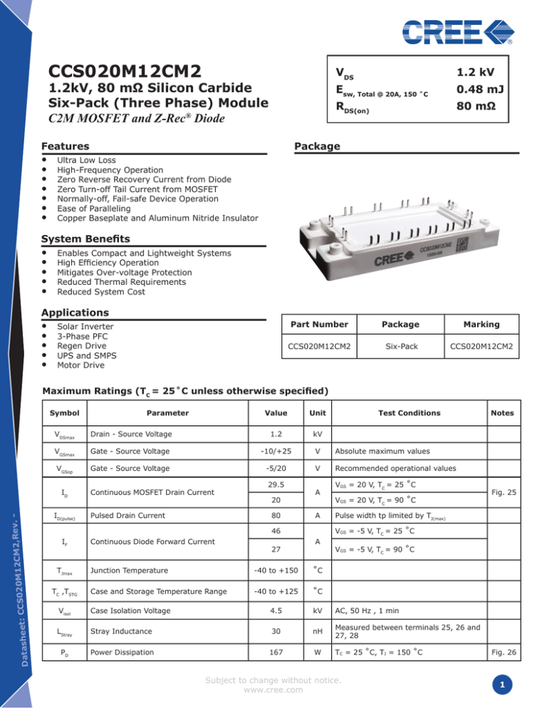
CCS020M12CM2
1.2kV, 80 mΩ Silicon Carbide
Six-Pack (Three Phase) Module
C2M MOSFET and Z-Rec® Diode
1.2 kV
RDS(on)
80 mΩ
Esw, Total @ 20A, 150 ˚C
Features
•
•
•
•
•
•
•
VDS
0.48 mJ
Package
Ultra Low Loss
High-Frequency Operation
Zero Reverse Recovery Current from Diode
Zero Turn-off Tail Current from MOSFET
Normally-off, Fail-safe Device Operation
Ease of Paralleling
Copper Baseplate and Aluminum Nitride Insulator
System Benefits
•
•
•
•
•
Enables Compact and Lightweight Systems
High Efficiency Operation
Mitigates Over-voltage Protection
Reduced Thermal Requirements
Reduced System Cost
Applications
•
•
•
•
•
Solar Inverter
3-Phase PFC
Regen Drive
UPS and SMPS
Motor Drive
Part Number
Package
Marking
CCS020M12CM2
Six-Pack
CCS020M12CM2
Maximum Ratings (TC = 25˚C unless otherwise specified)
Symbol
2,Rev. -
Value
Unit
Test Conditions
VDSmax
Drain - Source Voltage
1.2
kV
VGSmax
Gate - Source Voltage
-10/+25
V
Absolute maximum values
VGSop
Gate - Source Voltage
-5/20
V
Recommended operational values
ID
S020M12CM
Datasheet: CC
Parameter
ID(pulse)
Continuous MOSFET Drain Current
Pulsed Drain Current
29.5
20
80
A
A
46
IF
TJmax
TC ,TSTG
Continuous Diode Forward Current
27
A
Junction Temperature
-40 to +150
˚C
Case and Storage Temperature Range
-40 to +125
˚C
VGS = 20 V, TC = 25 ˚C
VGS = 20 V, TC = 90 ˚C
Notes
Fig. 25
Pulse width tp limited by TJ(max)
VGS = -5 V, TC = 25 ˚C
VGS = -5 V, TC = 90 ˚C
Visol
Case Isolation Voltage
4.5
kV
AC, 50 Hz , 1 min
LStray
Stray Inductance
30
nH
Measured between terminals 25, 26 and
27, 28
PD
Power Dissipation
167
W
TC = 25 ˚C, TJ = 150 ˚C
Subject to change without notice.
www.cree.com
Fig. 26
1
Electrical Characteristics (TC = 25˚C unless otherwise specified)
Symbol
Parameter
Min.
V(BR)DSS
Drain - Source Breakdown Voltage
VGS(th)
Gate Threshold Voltage
Typ.
Max.
1.2
1.7
Unit
kV
2.2
V
1.6
Test Conditions
VGS, = 0 V, ID = 100 µA
VDS = 10 V, ID = 1 mA
Zero Gate Voltage Drain Current
1
100
μA
VDS = 1.2 kV, VGS = 0V
IDSS
Zero Gate Voltage Drain Current
10
250
μA
VDS = 1.2 kV, VGS = 0V,TJ = 150 ˚C
IGSS
Gate-Source Leakage Current
1
250
nA
VGS = 20 V, VDS = 0V
On State Resistance
80
98
145
208
9.8
mΩ
VGS = 20 V, IDS = 20 A
Fig.
4-6
VGS = 20 V, IDS = 20 A, TJ = 150 ˚C
VDS = 20 V, IDS = 20 A
gfs
Transconductance
Ciss
Input Capacitance
900
Coss
Output Capacitance
181
Crss
Reverse Transfer Capacitance
5.9
Eon
Turn-On
Switching Energy 0.41
mJ
EOff
Turn-Off Switching Energy 0.07
mJ
3.8
Ω
f = 1 MHz, VAC = 25 mV
nC
VDD= 800 V, VGS = -5V/+20V,
ID= 20 A, Per JEDEC24 pg 27
Fig. 15
VDD = 800V, VGS = -5/+20V,
ID = 20 A, RG(ext) = 2.5 Ω,
Timing relative to VDS
Note: IEC 60747-8-4, pg 83
Resistive load
Fig. 24
IF = 20 A, VGS = 0, TJ = 25 ˚C
Fig. 10
IF = 20 A, VGS = 0, TJ = 150 ˚C
Fig. 11
RG (int)
S
Fig. 7
VDS = 10 V, ID = 1 mA, TJ = 150 ˚C
IDSS
RDS(on)
Note
8.5
Internal Gate Resistance
pF
QGS
Gate-Source Charge
16.1
QGD
Gate-Drain Charge
20.7
QG
Total Gate Charge
61.5
td(on)
Turn-on delay time
10
ns
tr(on)
VSD fall time 90% to 10%
td(off)
Turn-off delay time
tf(off)
VSD rise time 10% to 90%
VSD
Diode Forward Voltage
QC
Total Capacitive Charge
14
ns
22.4
ns
53
ns
1.5
1.7
1.8
2.3
0.27
V
μC
Fig. 8
VDS = 20 V, ID = 20 A, TJ = 150 ˚C
VDS = 800 V, f = 1 MHz,
VAC = 25 mV
Fig.
16,17
VDD = 800 V, VGS = -5V/+20V
ID = 20 A, RG(ext) = 2.5 Ω
Load = 412 μH, TJ = 150 ˚C
Note: IEC 60747-8-4 Definitions
Fig. 22
ISD = 20 A, VDS = 800V
di/dt = 1500 A/μs, VGS = -5V
Thermal Characteristics
Symbol
Parameter
Min.
Typ.
Max.
RthJCM
Thermal Resistance Juction-to-Case for MOSFET
0.7
0.75
RthJCD
Thermal Resistance Juction-to-Case for Diode
0.8
0.85
Unit
Test Conditions
Note
Fig. 27
˚C/W
Fig. 28
Additional Module Data
Symbol
Condition
Unit
Test Condition
W
Weight
180
g
M
Mounting Torque
5.0
Nm
To Heatsink and terminals
14.09
mm
Terminal to terminal
14.11
mm
Terminal to terminal
17.46
mm
Terminal to baseplate
Clearance Distance
Creepage Distance
2
Max.
CCS020M12CM2,Rev. -
Typical Performance
50
Drain-Source Current, IDS (A)
60
Conditions:
TJ = -40 °C
tp < 200 µs
Conditions:
TJ = 25 °C
tp < 200 µs
VGS = 20 V
50
VGS = 16 V
VGS = 18 V
Drain-Source Current, IDS (A)
60
VGS = 14 V
40
VGS = 12 V
30
20
VGS = 10 V
10
VGS = 20 V
VGS = 18 V
40
VGS = 12 V
30
VGS = 10 V
20
10
0
0
1
2
3
4
5
6
7
8
9
0
10
0
1
2
3
Drain-Source Voltage, VDS (V)
60
5
6
7
8
9
10
Figure 2. Output Characteristics TJ = 25 ˚C
2.0
Conditions:
TJ = 150 °C
tp < 200 µs
50
4
Drain-Source Voltage, VDS (V)
Figure 1. Output Characteristics TJ = -40 ˚C
VGS = 16 V
1.6
VGS = 18 V
40
Conditions:
IDS = 20 A
VGS = 20 V
tp < 200 µs
1.8
VGS = 14 V
VGS = 20 V
On Resistance, RDS On (P.U.)
Drain-Source Current, IDS (A)
VGS = 14 V
VGS = 16 V
VGS = 12 V
VGS = 10 V
30
20
10
1.4
1.2
1.0
0.8
0.6
0.4
0.2
0.0
0
0
1
2
3
4
5
6
7
8
9
-50
10
-25
0
TJ = 150 °C
150
100
TJ = 25 °C
TJ = -40 °C
50
100
125
150
140
120
VGS = 14 V
100
VGS = 16 V
VGS = 18 V
80
VGS = 20 V
60
40
20
0
0
0
10
20
30
40
50
Drain-Source Current, IDS (A)
Figure 5. On-Resistance vs. Drain Current
For Various Temperatures
3
75
Conditions:
IDS = 20 A
tp < 200 µs
160
On Resistance, RDS On (mOhms)
On Resistance, RDS On (mOhms)
180
Conditions:
VGS = 20 V
tp < 200 µs
200
50
Figure 4. Normalized On-Resistance vs. Temperature
Figure 3. Output Characteristics TJ = 150 ˚C
250
25
Junction Temperature, TJ (°C)
Drain-Source Voltage, VDS (V)
CCS020M12CM2,Rev. -
60
-50
-25
0
25
50
75
100
125
Junction Temperature, TJ (°C)
Figure 6. On-Resistance vs. Temperature
for Various Various Gate-Source Voltages
150
Typical Performance
3.5
2.5
2.0
1.5
1.0
0.5
30
TJ = 150 °C
25
TJ = 25 °C
20
15
TJ = -40 °C
10
5
0.0
-50
-25
0
25
50
75
100
125
0
150
0
Junction Temperature TJ (°C)
-2.5
-2.0
-1.5
-1.0
-0.5
0.0
6
8
10
12
-3.5
-3.0
-2.5
-1.5
-2.0
-1.0
-0.5
0
Condition:
TJ = -40 °C
tp < 200 µs
Drain-Source Current, IDS (A)
4
14
Figure 8. Transfer Characteristic for Various
Junction Temperatures
-10
-20
VGS = -2 V
-30
VGS = -5 V
-40
-50
0.0
0
Condition:
TJ = 25 °C
tp < 200 µs
Drain-Source Current, IDS (A)
-3.0
2
Gate-Source Voltage, VGS (V)
Figure 7. Threshold Voltage vs. Temperature
-3.5
Conditions:
VDS = 20 V
tp < 200 µs
35
Drain-Source Current, IDS (A)
3.0
Threshold Voltage, Vth (V)
40
Conditons
VDS = 10 V
IDS = 1 mA
-10
-20
VGS = -2 V
-30
VGS = -5 V
-40
VGS = 0 V
-50
VGS = 0 V
-60
-60
Drain-Source Voltage, VDS (A)
Drain-Source Voltage, VDS (A)
Figure 10. Diode Characteristic at 25 ˚C
Figure 9. Diode Characteristic at -40 ˚C
-3.0
-2.5
-2.0
-1.5
-1.0
-0.5
Drain-Source Current, IDS (A)
Condition:
TJ = 150 °C
tp < 200 µs
-3.0
0.0
VGS = -2 V
-30
VGS = 0 V
-2.0
-1.5
-1.0
-0.5
0.0
0
Conditions:
TJ = -40 °C
tp < 200 µs
-10
-20
VGS = -5 V
-2.5
0
-40
Drain-Source Current, IDS (A)
-3.5
VGS = 0 V
-10
VGS = 5 V
VGS = 10 V
-30
VGS = 20 V
-40
-50
-60
Drain-Source Voltage, VDS (A)
Figure 11. Diode Characteristic at 150 ˚C
4
CCS020M12CM2,Rev. -
-20
VGS = 15 V
-50
Drain-Source Voltage, VDS (V)
Figure 12. 3rd Quadrant Characteristic at -40 ˚C
-60
Typical Performance
-3.0
-2.5
-2.0
-1.5
-1.0
-0.5
-3.5
0.0
-3.0
-2.5
-2.0
-1.5
-1.0
-0.5
0.0
0
0
Conditions:
TJ = 25 °C
tp < 200 µs
Conditions:
TJ = 150 °C
tp < 200 µs
VGS = 0 V
Drain-Source Current, IDS (A)
VGS = 5 V
-20
VGS = 15 V
-30
VGS = 20 V
-40
Drain-Source Current, IDS (A)
-10
VGS = 10 V
VGS = 0 V
-10
VGS = 5 V
VGS = 20 V
VGS = 10 V
-20
VGS = 15 V
-30
-40
-50
-50
-60
Drain-Source Voltage, VDS (V)
Figure 14. 3rd Quadrant Characteristic at 150 ˚C
Figure 13. 3rd Quadrant Characteristic at 25 ˚C
25
10000
Conditions:
IDS = 20 A
IGS = 100 mA
VDS = 800 V
TJ = 25 °C
20
1000
15
10
5
Coss
100
10
Crss
0
-5
0
Conditions:
TJ = 25 °C
VAC = 25 mV
f = 1 MHz
Ciss
Capacitance (pF)
Gate-Source Voltage, VGS (V)
-60
Drain-Source Voltage, VDS (V)
10
20
30
40
50
60
1
70
0
Gate Charge, QG (nC)
150
200
120
Conditions:
TJ = 25 °C
VAC = 25 mV
f = 1 MHz
Ciss
100
Drain-Source Voltage, VDS (V)
Figure 16. Capacitances vs. Drain-Source
Voltage (0 - 200 V)
Figure 15. Gate Charge Characteristics
10000
50
100
100
Stored Energy, EOSS (µJ)
Capacitance (pF)
1000
Coss
10
1
200
400
600
Drain-Source Voltage, VDS (V)
800
Figure 17. Capacitances vs. Drain-Source
Voltage (0 - 1 kV)
5
CCS020M12CM2,Rev. -
60
40
20
Crss
0
80
1000
0
0
200
400
600
800
1000
Drain to Source Voltage, VDS (V)
Figure 18. Output Capacitor Stored Energy
1200
Typical Performance
0.25
Switching Energy (mJ)
0.8
Conditions:
TJ = 25 °C
VDD = 600 V
RG(ext) = 2.5 Ω
VGS = -5/+20 V
L = 412 μH
0.2
Conditions:
TJ = 25 °C
VDD = 800 V
RG(ext) = 2.5 Ω
VGS = -5/+20 V
L = 412 μH
0.7
ETotal
0.6
Switching Energy (mJ)
0.3
EOn
0.15
0.1
EOff
0.05
ETotal
0.5
EOn
0.4
0.3
0.2
EOff
0.1
0
0
0
5
10
15
20
25
30
35
40
45
0
5
10
Drain to Source Current, IDS (A)
Figure 19. Inductive Switching Energy vs.
Drain Current For VDS = 600V
Switching Loss (mJ)
1.0
35
40
45
Conditions:
IDS = 20 A
VDD = 800 V
RG(ext) = 2.5 Ω
VGS = -5/+20 V
L = 412 µH
0.6
EOn
0.8
0.6
0.4
0.5
ETotal
0.4
EOn
0.3
0.2
EOff
0.1
0.0
EOff
0.0
0
10
20
30
40
50
0
25
50
External Gate Resistor RG(ext) (Ohms)
120
Conditions:
TJ = 25 °C
RG(ext) = 2.5 Ω
IDS = 20 A
VGS = -5/+20 V
L = 412 μH
0.8
0.7
0.6
100
125
150
175
Figure 22. Inductive Switching Energy vs.
Temperature
Conditions:
TJ = 25 °C
VDD = 800 V
RL = 40 Ω
VGS = -5/+20 V
100
ETotal
80
0.5
Time (ns)
0.9
75
Junction Temperature, TJ (°C)
Figure 21. Inductive Switching Energy
vs. RG(ext)
Switching Loss (mJ)
30
0.7
ETotal
0.2
EOn
0.4
60
tf
40
0.3
0.2
td (off)
tr
20
EOff
0.1
td (on)
0
0.0
300
400
500
600
700
800
900
Drain to Source Voltage, VDS (V)
Figure 23. Inductive Switching Energy vs.
VDS
6
25
0.8
Conditions:
TJ = 25 °C
VDD = 800 V
IDS = 20 A
VGS = -5/+20 V
L = 412 μH
1.2
20
Figure 20. Inductive Switching Energy vs.
Drain Current For VDS = 800V
Swithcing Loss (mJ)
1.4
15
Drain to Source Current, IDS (A)
CCS020M12CM2,Rev. -
1000
0
5
10
15
20
25
30
35
External Gate Resistor, RG(ext) (Ohms)
Figure 24. Timing vs. RG(ext)
40
45
50
Typical Performance
180
Conditions:
TJ ≤ 150 °C
45
Maximum Dissipated Power, Ptot (W)
Drain-Source Continous Current, IDS (DC) (A)
50
40
35
30
25
20
15
10
5
0
Conditions:
TJ ≤ 150 °C
160
140
120
100
80
60
40
20
0
-40
-20
0
20
40
60
80
100
120
140
-40
-20
0
20
Figure 25. Continuous Drain Current Derating vs.
Case Temperature
60
80
100
120
1
Junction To Case Impedance, ZthJC (oC/W)
0.5
0.3
100E-3
0.5
0.3
100E-3
0.1
0.05
0.02
SinglePulse
10E-3
0.01
1E-3
0.1
0.05
0.02
10E-3
SinglePulse
0.01
1E-3
1E-6
10E-6
100E-6
1E-3
10E-3
Time, tp (s)
100E-3
1
10
Figure 27. MOSFET Junction to Case Thermal Impedance
1E-6
10E-6
100E-6
1E-3
10E-3
Time, tp (s)
100E-3
1
10
Figure 28. Diode Junction to Case Thermal Impedance
100.00
100000
10 µs
Drain-Source Current, IDS (A)
NTC Resistance (Ohms)
Limited by RDS On
10000
1000
100
10
-50
-25
0
25
50
75
100
125
NTC Temperature (°C)
Figure 29. NTC Resistance vs NTC Temperature
7
140
Figure 26. Maximum Power Dissipation (MOSFET)
Derating vs Case Temperature
1
Junction To Case Impedance, ZthJC (oC/W)
40
Case Temperature, TC (°C)
Case Temperature, TC (°C)
CCS020M12CM2,Rev. -
150
100 µs
10.00
1 ms
100 ms
1.00
0.10
Conditions:
TC = 25 °C
D = 0,
Parameter: tp
0.01
0.1
1
10
100
1000
Drain-Source Voltage, VDS (V)
Figure 30. MOSFET Safe Operating Area
Figure 31. Resistive Switching Time Description
NTC Characteristics
Symbol
R25
Delta R/R
P25
Condition
TC = 25 °C
Typ.
Max.
5
Unit
kΩ
TC = 100 °C, R100 = 481 Ω
±5
%
TC = 25 °C
20
mW
B25/50
R2 = R25 exp[B25/50(1/T2-1/(298.15K))]
3380
K
B25/80
R2 = R25 exp[B25/80(1/T2-1/(298.15K))]
3440
K
8
CCS020M12CM2,Rev. -
Schematic
Package Dimensions (mm)
CCS020M12CM2
9
CCS020M12CM2,Rev. -
Notes
• RoHS Compliance
The levels of RoHS restricted materials in this product are below the maximum concentration values (also referred
to as the threshold limits) permitted for such substances, or are used in an exempted application, in accordance
with EU Directive 2011/65/EC (RoHS2), as implemented January 2, 2013. RoHS Declarations for this product can
be obtained from your Cree representative or from the Product Documentation sections of www.cree.com.
• REACh Compliance
REACh substances of high concern (SVHCs) information is available for this product. Since the European Chemical Agency (ECHA) has published notice of their intent to frequently revise the SVHC listing for the foreseeable
future,please contact a Cree representative to insure you get the most up-to-date REACh SVHC Declaration.
REACh banned substance information (REACh Article 67) is also available upon request.
•
This product has not been designed or tested for use in, and is not intended for use in, applications implanted into
the human body nor in applications in which failure of the product could lead to death, personal injury or property
damage, including but not limited to equipment used in the operation of nuclear facilities, life-support machines,
cardiac defibrillators or similar emergency medical equipment, aircraft navigation or communication or control
systems, air traffic control systems.
Module Application Note:
The SiC MOSFET module switches at speeds beyond what is customarily associated with IGBT based modules.
Therefore, special precautions are required to realize the best performance. The interconnection between the gate
driver and module housing needs to be as short as possible. This will afford the best switching time and avoid the
potential for device oscillation. Also, great care is required to insure minimum inductance between the module and
link capacitors to avoid excessive VDS overshoots.
Please Refer to application note: Design Considerations when using Cree SiC Modules Part 1 and Part 2.
[CPWR-AN12, CPWR-AN13]
Copyright © 2014 Cree, Inc. All rights reserved.
The information in this document is subject to change without notice.
Cree, the Cree logo, and Zero Recovery are registered trademarks of Cree, Inc.
10
CCS020M12CM2 Rev -
Cree, Inc.
4600 Silicon Drive
Durham, NC 27703
USA Tel: +1.919.313.5300
Fax: +1.919.313.5451
www.cree.com/power


