Thermal Characterization and Board Level Modeling
of the RSLIC18 in the MLFP Package
TM
Application Note
October 2001
AN9922
Author: Doug Bruss
Introduction
In most circuit designs realestate is a premium. This is
especially true for the new
generation of Home
Gateway and Remote
Terminal voice circuits, where some solutions allocate less
than one square inch for the SLIC and its components. With
the development of Quad and Octal CODECS the SLIC now
has a larger share of the solutions real-estate and a larger
impact on area reduction. Small packaging has been around
for some time, but there has not been a reliable, cost
effective solution to significantly reduce the SLIC’s area until
now. The most significant hurdle has been the power
dissipation capability of the package, which has been
addressed with a new “Micro Lead Frame” Package
technology. The improved thermal dissipation performance
comes from the exposed lead frame that is used to help pull
heat out of the die with the aid of thermal vias that tie directly
to a heat sink plane. With this new technology Designers can
take advantage of a 65% reduction in the RSLIC18’s
footprint (7mm x 7mm) and realize a significant improvement
in thermal performance.
The Micro Lead Frame Plastic Package (MLFP) is a JEDEC
standard package outline (EIA/JEDEC Publication 95, MO220) and has several aliases. For example, depending on
the manufacturer it may be referred to as a “Micro Lead
Frame (MLF), a “Quad Flat No Lead Package” (QFN), or a
“Lead Frame Chip Scale Package” (LFCSP).
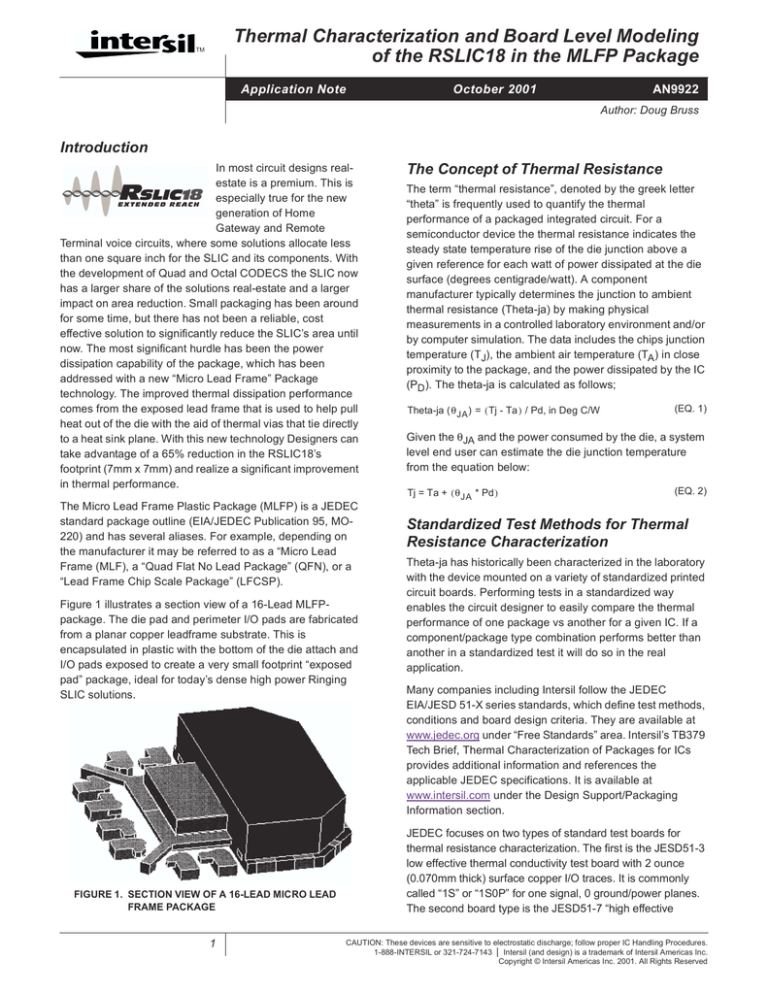
Figure 1 illustrates a section view of a 16-Lead MLFPpackage. The die pad and perimeter I/O pads are fabricated
from a planar copper leadframe substrate. This is
encapsulated in plastic with the bottom of the die attach and
I/O pads exposed to create a very small footprint “exposed
pad” package, ideal for today’s dense high power Ringing
SLIC solutions.
FIGURE 1. SECTION VIEW OF A 16-LEAD MICRO LEAD
FRAME PACKAGE
1
The Concept of Thermal Resistance
The term “thermal resistance”, denoted by the greek letter
“theta” is frequently used to quantify the thermal
performance of a packaged integrated circuit. For a
semiconductor device the thermal resistance indicates the
steady state temperature rise of the die junction above a
given reference for each watt of power dissipated at the die
surface (degrees centigrade/watt). A component
manufacturer typically determines the junction to ambient
thermal resistance (Theta-ja) by making physical
measurements in a controlled laboratory environment and/or
by computer simulation. The data includes the chips junction
temperature (TJ), the ambient air temperature (TA) in close
proximity to the package, and the power dissipated by the IC
(PD ). The theta-ja is calculated as follows;
Theta-ja (θ JA ) = ( Tj - Ta ) / Pd, in Deg C/W
(EQ. 1)
Given the θJA and the power consumed by the die, a system
level end user can estimate the die junction temperature
from the equation below:
Tj = Ta + ( θ JA * Pd )
(EQ. 2)
Standardized Test Methods for Thermal
Resistance Characterization
Theta-ja has historically been characterized in the laboratory
with the device mounted on a variety of standardized printed
circuit boards. Performing tests in a standardized way
enables the circuit designer to easily compare the thermal
performance of one package vs another for a given IC. If a
component/package type combination performs better than
another in a standardized test it will do so in the real
application.
Many companies including Intersil follow the JEDEC
EIA/JESD 51-X series standards, which define test methods,
conditions and board design criteria. They are available at
www.jedec.org under “Free Standards” area. Intersil’s TB379
Tech Brief, Thermal Characterization of Packages for ICs
provides additional information and references the
applicable JEDEC specifications. It is available at
www.intersil.com under the Design Support/Packaging
Information section.
JEDEC focuses on two types of standard test boards for
thermal resistance characterization. The first is the JESD51-3
low effective thermal conductivity test board with 2 ounce
(0.070mm thick) surface copper I/O traces. It is commonly
called “1S” or “1S0P” for one signal, 0 ground/power planes.
The second board type is the JESD51-7 “high effective
CAUTION: These devices are sensitive to electrostatic discharge; follow proper IC Handling Procedures.
1-888-INTERSIL or 321-724-7143 | Intersil (and design) is a trademark of Intersil Americas Inc.
Copyright © Intersil Americas Inc. 2001. All Rights Reserved
Application Note AN9922
thermal conductivity” board, and is more applicable for today’s
multi layer PCBs. It adds two continuous, one ounce
(0.035mm) buried copper planes, and is usually called 1S2P
indicating 1 signal (top) and two buried planes. JEDEC has
recently added the JESD51-5 “extension” standard for
packages with direct thermal attachment mechanisms. This
spec provides for surface attachment pads and copper
plated thermal vias that connect directly to the upper buried
plane of the 1S2P board. This new board type is called the
1S2P-DA where the “DA” stands for “direct attach”. It applies
to exposed pad packages such as SOIC, TSSOP, TQFP, and
the MLFP.
Power Estimates for Worst Case
Conditions
It is important to understand the maximum power the SLIC is
expected to dissipate in a given application to ensure safe
and reliable operating conditions are met. As noted in the
HC5518X data sheets the maximum recommended
operating temperature is 150oC. The device also has a
temperature sensing circuit on board that will power down
the SLIC when the junction temperature exceeds 170oC. A
Power Spread sheet is available on the Intersil Web site to
assist the designer with this estimate. It can be accessed at
www.intersil.com under VoIP Applications.
The worst case scenarios for power consumption are short
loop applications. Off-hook operation also referred to as the
“Talk Mode” (Forward Active), and Ringing (multiple phones)
should be considered. When quantifying the power
consumption during ringing, one must factor in the ring
cadence which is typically (two seconds ringing, four
seconds idle). For example, when ringing 5 phones
continuously with a maximum peak-to-peak waveform
(190V) the power consumed by the SLIC can exceed 1.25W,
however with a ringing cadence of two seconds ringing, four
seconds idle the power is reduced to 0.6W. When the
transient power pulse (2sec) and the period (6sec) are
relatively short as is the case for ringing the phone, the
average power and the θJA can be used to accurately
predict the Die’s junction temperature. Typically the off hook
talk mode is the worst case, and under short loop conditions
the SLIC will consume 400 to 500mW.
2
Thermal Characterization in the MLFP
Package
Advancements in thermal modeling have made simulation
the preferred method for thermal characterization. With the
development and use of Finite Element Analysis (FEA)
software, correlation to within 4-8% is routinely achieved
between the simulator and laboratory data. Once this very
good level of correlation is obtained with the standard
JEDEC test boards multiple simulations are performed to
generate the data shown in Figures 2 and 3.
Figure 2 summarizes the θja of the 32 pin MLFP package for
the three JEDEC standard test boards for the RSLIC18.
Note that without buried planes or thermal vias the package
can’t dissipate heat effectively (78oC/W, 1SOP) which would
significantly limit the application. Adding the buried planes
and connecting to the upper plane with conductive vias
(1S2P-DA) significantly reduces the θja to less than 30oC/W
(1S2P-DA). Keep in mind that the area of each internal
buried plan is 2.92 x 2.92 inches on the test boards and
essentially represents an infinite heat sink.
Figure 3 illustrates the effect of various heat sink areas on
the θJA of the HC55185 using the 1S2P-DA test board with
thermal vias. This data-set is more applicable for the
designer as one can probably assume the MLFP package is
being used to realize a dense line circuit solution and the
heat sink area will be restricted. The data shows that θJA’s of
less than 50oC/W can be expected with less than one
square inch of heat sink area dedicated to the SLIC.
The question that now comes to mind is how do adjacent
SLICs interact thermally and what effect does the heat sink
plane have on the overall board temperature in a dense line
card application? We can simulate these interactions and
predict the maximum die and circuit board temperatures with
a relatively simple board level model. Figure 4 illustrates the
board layout and defines the conditions for the thermal
simulations depicted in Figures 5, 6 and 7. For each
simulation the SLICs were spaced one inch apart (center to
center) in a 4 by 6 array resulting in a packing density of one
square inch per device. All units are dissipating 500mW in
the Forward Active loop feed mode (talk mode). Note that
the only variable changed in the simulations was the area of
the heat sink plane. To keep the simulations manageable the
model was set up without any top level interconnects
representing a worse case condition for thermal conductivity.
Application Note AN9922
80
78
120
110
70
100
50
41
40
30
27
THETA-JA (oC/W)
THETA-JA (oC/W)
60
90
80
70
60
50
20
40
10
30
20
0
0
1
1S2P
1S2P-DA (vias)
1S0P
JEDEC THERMAL TEST BOARD TYPE
FIGURE 2. MLFP 7x7, 32-LEAD, THETA-JA vs BOARD TYPE
2
3
4
5
6
7
8
9
10
BURIED PLANE AREA (SQUARE INCH)
FIGURE 3. MLFP 7x7, 32 LEAD, THETA-JA vs BURIED
PLANE AREA (IS2P-DA)
NOTES:
1. Assumes natural convection, board horizontal.
2. “DA” board includes “Direct Attach” thermal vias (16 at 0.3mm drill diameter) per JESD 51-5.
3. In all cases, the package die pad is soldered to the matching board pad.
4. Board metal thickness 100% thick 2 ounce signal, and 95% thick 1 ounce buried copper planes).
MLFP Package Details
7x7mm-32-pin, 5.3mm pad top, 5.1mm pad bottom.
Board Details:
A 3x4.5” 1S2P-DA (“direct attach”) board type with two 1
ounce Cu buried planes and 16 vias connecting to the upper
plane only (per JEDEC).
On the board surface, traces fan out radially from the
surface. As the plane size is decreased, the 2 ounce surface
trace lengths are also decreased so that the traces end
slightly inside of the plane size. For the 1/4 x 1/4 inch plane,
trace lengths are the same as for the 1/2 x 1/2 inch plane
(otherwise there would be no traces, they would be too
short).
HC55185 MLF THERMAL MODELING APPLICATION BOARD
• Units spaced 1 inch apart (center to center)
• Heat sink area = 1 sq inch per device
• All devices active and dissipating 500mW
• Board thickness = 1.6mm
• Buried planes = 1oz copper
• Copper thickness = 0.035mm
• FR4 thickness = 0.375mm top/bottom to buried
plane
• FR4 thickness = 0.78mm between buried planes
• 16 conductive thermal vias tied to the upper
buried plane
FIGURE 4. BOARD SIZE = 8 INCHES x 12 INCHES WITH VARIOUS HEAT SINK PLANES
3
Application Note AN9922
Simulation #1 (Figure 5) restricts to heat sink plan to the
area directly under the 4 x 6 array of SLICs creating an
effective heat sink area of 1 square inch/device. With an
ambient temperature of 25oC the maximum die temperature
reaches 73oC for most units and the board temperature in
close proximity to the hottest units reaches approximately
65oC. In this instance the heat sink plane is saturated
resulting in an effective θJA of 96oC/W. Increasing the
ambient temperature to 85oC would result in a maximum die
temperature of 133oC which is well within the safe operating
temperature range of the SLIC (Max = 150oC). Note that the
FR4 material is an excellent thermal barrier which could be
beneficial for heat sensitive components.
Simulation #2 (Figure 6) increases the heat sink plane to
8 inches x 8 inches providing additional heat sink area to the
units on the perimeter of the array. At 25oC ambient, the
maximum die temperature of 67oC is observed on the units
in the two center rows. The additional heat sink area reduces
the effective θJA on these devices to 84oC/W. Increasing the
ambient temperature to 85oC would result in a maximum die
temperature of 127oC.
Simulation #3 (Figure 7) shows the effect of increasing the
heat sink plane to match the total board area of
8 inches x 12 inches. In this case the additional heat sink
area provides little if any improvement in thermal
conductivity for the units in the center rows. This suggests
that the packing density of one square inch per unit limits the
effective θJA to approximately 84oC/W for units in the center
of the array.
These simulations indicate the heat sink plane can saturate
when packing densities are pushed to the extreme, however
the resulting θJA’s are more than adequate to keep the
device well under the maximum die temperature of 150oC
when operating at 85oC ambient.
ALL UNITS DISSIPATING 0.5W
TJ(MAX) = 73 oC = 25oC + TJA * 0.5W
TJA (EFFECTIVE) = 48/.5 = 96oC/W
TJ @ 85oC = 85 oC + 0.5W * 96oC/W = 133oC
TEMPERATURE
25
27
29
31
33
35
37
39
41
43
45
47
49
51
53
55
57
59
61
63
65
67
69
71
73
FIGURE 5. HC55185 BOARD LEVEL THERMAL ANALYSIS WITH TOW 4 X 6 INCH BURIED PLANES
4
Application Note AN9922
ALL UNITS DISSIPATING 0.5W
TJ(MAX) = 67oC = 25 oC + (TJA * 0.5W)
TJA (EFFECTIVE) = 42/.5 = 84oC/W
TJ @ 85oC = 85oC + 0.5W * 84oC/W = 127 oC
TEMPERATURE
25
27
29
31
33
35
37
39
41
43
45
47
49
51
53
55
57
59
61
63
65
67
69
71
73
FIGURE 6. HC55185 BOARD LEVEL THERMAL ANALYSIS WITH TWO 8 x 8 INCH BURIED PLANES
ALL UNITS DISSIPATING 0.5W
TJ(MAX) = 67 oC = 25oC + (TJA * 0.5W)
TJA (EFFECTIVE) = 42/.5 = 84oC/W
TJ @ 85oC = 85 oC + (0.5W * 84 oC/W) = 127oC
TEMPERATURE
25
27
29
31
33
35
37
39
41
43
45
47
49
51
53
55
57
59
61
63
65
67
69
71
73
FIGURE 7. HC55185 BOARD LEVEL THERMAL ANALYSIS WITH TWO 8 x 12 INCH BURIED PLANES
5
Application Note AN9922
Figure 8 further illustrates the impact of device spacing
(pitch) on the effective theta-ja. This graph summarizes the
results of 8 simulations where the pitch on an infinite matrix
of RSLIC18’s is varied from .5 inches to 2.92 inches in .25
inch increments. Note the substantial reduction in effective
theta-ja that is obtained with only slight increases in device
pitch.
280
274
ON 1S2P-DA(VIA) BOARD
(WITH 5.3mm PAD, 4.58mm DIE)
260
240
Requirements and Recommendations for
Circuit Board Layout
• The lead-frame must be electrically tied to VBH . No
current flows through the substrate so a current limiting
resistor in the order of 100K can be implemented to
address any safety issues.
• The electrical connection of the heat sink plane to VBH
should be made on the cathode side of the VBH protection
diode.
• Dedicate an internal power plane to spread the heat and
optimize thermal dissipation.
220
• Make the heat sink plane as large as possible to minimize
board and die temperature. Effective heat sink areas of 1
sq inch/device are acceptable.
THETA-JA (Co/W)
200
180
160
153
• Use conductive copper plated vias to make the electrical
and thermal tie to the heat sink plane.
140
120
99.5
100
71.5
55.6
80
60
45.7
39.1
40
28.0
20
0
0
0.25 0.5 0.75 1.0 1.25 1.5 1.75 2.0 2.25 2.5 2.75 3.0
MATRIX PITCH (INCHES)
FIGURE 8. THETA-JA vs MATRIX PITCH FOR LARGE
SQUARE MATRIX OF 32 PIN 7x7mm MLFPs
All Intersil products are manufactured, assembled and tested utilizing ISO9000 quality systems.
Intersil Corporation’s quality certifications can be viewed at www.intersil.com/design/quality
Intersil products are sold by description only. Intersil Corporation reserves the right to make changes in circuit design, software and/or specifications at any time without
notice. Accordingly, the reader is cautioned to verify that data sheets are current before placing orders. Information furnished by Intersil is believed to be accurate and
reliable. However, no responsibility is assumed by Intersil or its subsidiaries for its use; nor for any infringements of patents or other rights of third parties which may result
from its use. No license is granted by implication or otherwise under any patent or patent rights of Intersil or its subsidiaries.
For information regarding Intersil Corporation and its products, see www.intersil.com
Sales Office Headquarters
NORTH AMERICA
Intersil Corporation
7585 Irvine Center Drive
Suite 100
Irvine, CA 92618
TEL: (949) 341-7000
FAX: (949) 341-7123
Intersil Corporation
2401 Palm Bay Rd.
Palm Bay, FL 32905
TEL: (321) 724-7000
FAX: (321) 724-7946
6
EUROPE
Intersil Europe Sarl
Ave. C - F Ramuz 43
CH-1009 Pully
Switzerland
TEL: +41 21 7293637
FAX: +41 21 7293684
ASIA
Intersil Corporation
Unit 1804 18/F Guangdong Water Building
83 Austin Road
TST, Kowloon Hong Kong
TEL: +852 2723 6339
FAX: +852 2730 1433
