ALM-1222
1.8-2.2GHz Low Noise, High Gain, High Linearity Balanced Amplifier Module
Data Sheet
Description
Features
Avago Technologies’ ALM-1222 is a very low noise, high
linearity balanced amplifier module operating in the 1.8
to 2.2GHz frequency range. The exceptional noise and
linearity performances are achieved through the use of
Avago Technologies’ proprietary 0.5um GaAs Enhancement-mode pHEMT process.
• Low noise figure
All matching components are fully integrated within
the module and the 50Ω RF input and output pins are
already internally AC-coupled. This makes the ALM-1222
extremely easy to use as the only external parts are DC
supply bypass capacitors.
The ALM-1222 is housed in a miniature 5.0 x 6.0 x 1.1
mm3 22-lead multiple-chips-on-board (MCOB) module
package. The compact footprint and low profile makes
this product an ideal choice for Wireless Infrastructure
Basestation Tower-Mounted Amplifiers (TMA), Radiocards and Multi-Carrier Driver Amplifiers in the cellular/
PCS/CDMA bands.
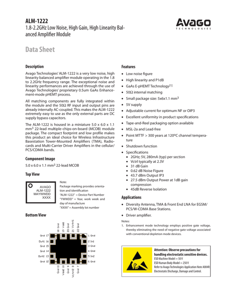
Component Image
5.0 x 6.0 x 1.1 mm3 22-lead MCOB
Top View
AVAGO
ALM-1222
MAYWWDD
XXXX
Bottom View
Note:
Package marking provides orientation and identification
“ALM-1222” = Device Part Number
“YWWDD” = Year, work week and
day of manufacture
“XXXX” = Assembly lot number
• High linearity and P1dB
• GaAs E-pHEMT Technology[1]
• 50Ω internal matching
• Small package size: 5x6x1.1 mm3
• 5V supply
• Adjustable current for optimum NF or OIP3
• Excellent uniformity in product specifications
• Tape-and-Reel packaging option available
• MSL-2a and Lead-free
• Point MTTF > 300 years at 120oC channel temperature
• Shutdown function
• Specifications
• 2GHz; 5V, 280mA (typ) per section
• Vctrl typically at 2.3V
• 31 dB Gain
• 0.62 dB Noise Figure
• 43.7 dBm Output IP3
• 27.5 dBm Output Power at 1dB gain
compression
• 45dB Reverse Isolation
Applications
• Diversity Antenna, TMA & Front End LNA for EGSM/
PCS/W-CDMA Base Stations.
• Driver amplifier.
Notes:
1. Enhancement mode technology employs positive gate voltage,
thereby eliminating the need of negative gate voltage associated
with conventional depletion mode devices.
Attention: Observe precautions for
handling electrostatic sensitive devices.
ESD Machine Model = 50 V
ESD Human Body Model = 250 V
Refer to Avago Technologies Application Note A004R:
Electrostatic Discharge, Damage and Control.
Absolute Maximum Rating [2] TA=25oC
Symbol
Parameter
Units
Absolute Max.
Vdd
Device Voltage, RF output to ground
V
5.5
Thermal Resistance [3](Vdd = 5.0V,
Vctrl=2.2V)qjc = 20 oC/W
Vctrl
Control Voltage
V
3.0
Notes:
Pin,max
CW RF Input Power
(Vdd = 5.0, Idd=280mA)
dBm
22
Pdiss
Total Power Dissipation [4]
W
5
2.
3.
4.
Tj
Junction Temperature
oC
150
TSTG
Storage Temperature
oC
-65 to 150
Operation of this device in excess of any of these limits may
cause permanent damage.
Thermal resistance measured
using Infra-Red measurement
technique.
Board (module belly) temperature TB is 25 oC.
Derate 50mW/oC for TB>95 oC.
Product Consistency Distribution Charts [5,6]
Process Capability for NF
150
Nominal = 0.62, USL = 1.0
Std dev=0.014
CPK>2
90
60
30
0.5
0.55
0.6
0.65
NF (dB)
0.7
Std dev=0.35
CPK=1.45
300
200
0
0.75
Figure 1. NF@ 2.0GHz; 5V, 280mA
Process Capability for OIP3
200
LSL = 39.0, Nominal = 43.7
120
Std dev=0.93
CPK=1.6
90
28.5 29 29.5 30 30.5 31 31.5 32 32.5 33
Gain (dB)
Figure 2. Gain @ 2.0GHz; 5V, 280mA
60
Process Capability for Vctrl
LSL = 1.9, Nominal = 2.3, USL = 2.8
Std dev = 0.07
CPK_L = 2.0
CPK_U = 2.1
160
frequency
150
frequency
LSL = 29.5, Nominal = 31.0
100
0
120
80
40
30
0
Process Capability for Gain
400
frequency
120
frequency
500
0
38
40
42
44
OIP3 (dBm)
Figure 3. OIP3@ 2.0GHz; 5V, 280mA
46
48
1.8
2
2.2
2.4
Vctrl (V)
2.6
2.8
Figure 4. Vctrl @ 2.0GHz; 5V, 280mA
Note:
5. Distribution data sample size is 500 samples taken from 3 different wafers and 3 different lots. Future wafers allocated to this product may have
nominal values anywhere between the upper and lower limits.
6. Measurements are made on a production test board, which can show a variance of up to 1dB in gain and OIP3 compared to a soldered-down
demo board. Input trace losses have been de-embedded from actual measurements.
Electrical Specifications [7], [10]
TA = 25 °C, Vdd =5V @ 280mA, RF performance at 2.0 GHz, given for each of the 2 RF paths, measured on demo board
(see Fig. 5) unless otherwise specified.
Symbol
Parameter and Test Condition
Vctrl
Control Voltage, Idd=280mA
Gain
Gain
OIP3 [8]
Units
Min.
Typ.
Max.
1.9
2.3
2.8
dB
29.5
31
32.5
Output Third Order Intercept Point
dBm
39
43.7
-
NF [9]
Noise Figure (Typ.Vctrl=2.2V)
dB
-
0.62
1.00
OP1dB
Output Power at 1dB Gain Compression
dBm
-
27.5
-
S11
Input Return Loss, 50W source
dB
-
-8
-
S22
Output Return Loss, 50W load
dB
-
-10
-
S12
Reverse Isolation
dB
-
45
-
ISO1-2
Isolation between RF Input 1 and RF Input 2
dB
-
22
-
Notes:
7. Measurements at 2GHz obtained using demo board described in Fig 5.
8. 2GHz OIP3 test condition: FRF1 = 2.0 GHz, FRF2 = 2.01 GHz with input power of -20dBm per tone measured at lower side band.
9. For NF data, board losses of 0.12dB at the input have been de-embedded.
10.Use proper bias, heatsink and derating to ensure maximum channel temperature is not exceeded. See absolute maximum ratings and application note for more details.
Demo Board Layout
Circuit
Symbol
Size
Description
C1, C10
0805
2.2uF ceramic
C2, C7
0402
Not used
C3, C6
0402
0.1uF ceramic
C4, C9
0402
Not used
C5, C8
0402
0.1uF ceramic
Ground
Pinout Designation
1
10
RF output 1
RF input 2
RF output 2
Recommended PCB material is 10 mils Rogers RO4350.
Suggested component values may vary according to
layout and PCB material.
Demo Board Schematic
Bias1
Vsense
3
21
20
1,2,19,20
Vsupply
8
Module outline
C3
1,22
C5
C1
19
17,18
Bias
50 --Ohms TL
Input
match
50 --Ohms TL
Interstage
match
16
Output
match
14,15
3,4
5
50 --Ohms TL
Input
match
Interstage
match
6
7
12
8
9
10
C6
11
Vsupply
Bias2
C8
10
13
Output
match
Bias
Figure 6. Demo Board Schematic Diagram
Vsuppyl
RF input 1
Figure 5. Demo Board Layout Diagram
2
20-pin connector
1,2,19,20
C10
50 --Ohms TL
1,2
Balanced Amplifier Demo Board Layout
Circuit
Symbol
Size
Description
C1, C10
0805
2.2uF ceramic
C2, C7
0402
Not used
C3, C6
0402
0.1uF ceramic
C4, C9
0402
Not used
C5, C8
0402
0.1uF ceramic
R1, R4
0402
Not used
R2, R3
0402
49.9 ohms
14.22x5.08
mm 2
Coupler
Ground
Anaren Xinger II
XC1900E -03 or equiv
20-pin connector
RF Input
RF Output
Figure 7. Suggested Balanced Amplifier Demo Board Layout
Recommended PCB material is 10 mils Rogers RO4350.
Suggested component values may vary according to
layout and PCB material.
Balanced Demo Board Schematic
1,2,19,20
Vsupply
Vctrl
Vsense
3
8
Module outline
C3
Coupler
C5
21
1,22
20
2
Input
match
Interstage
match
16
Output
match
14,15
5
50 -Ohms TL
Input
match
Interstage
match
6
12
Bias
7
8
9
10
11
Vsupply
Vctrl
C8
8
13
Output
match
C6
Figure 8. Application Schematic for Balanced Amplifier
R2
50 -Ohms TL
3,4
R3
Coupler
17,18
Bias
50 -Ohms TL
RF Input
C1
19
1,2,19,20
C10
50 -Ohms TL
RF Output
ALM-1222 Typical Performance I
TA = +25 oC, Vdd = 5V, Idd = 280mA Input Signal=CW unless stated otherwise.
1.6
31
1.4
29
1.2
27
1.0
25
0.8
0.6
23
21
-15
-20
-25
-30
-35
-40
0.2
17
-45
1.8
1.9
2.0
2.1
Freq (GHz)
2.2
15
2.3
1.7
1.8
1.9
2.0
2.1
Freq (GHz)
2.2
-50
2.3
Figure 10. Gain vs Frequency and channel
-15
S22 ch1
S22 ch2
-20
0
2
4
6
8 10 12 14 16 18 20
Freq (GHz)
Figure 12. S22 vs Frequency and channel
-50
1.0
0.8
0.4
0.
0
2
4
6
0.0
8 10 12 14 16 18 20
Freq (GHz)
1.7
33
31
40
31
9
35
9
7
30
7
1
19
15
1.7
1.8
1.9
.1
Freq (GHz)
.
0
15
10
-40˚C
5˚C
85˚C
17
OP1dB (dBm)
35
45
OIP3 (dBm)
50
33
5
Figure 15. Gain vs Frequency and temperature
1.7
1.8
1.9
.1
Freq (GHz)
.
.3
Figure 16. OIP3 vs Frequency and temperature
.
.3
5
3
1
-40˚C
5˚C
85˚C
17
0
.3
1.9
.1
Freq (GHz)
19
-40˚C
5˚C
85˚C
5
1.8
Figure 14. NF vs Frequency and temperature
35
3
-40˚C
5˚C
85˚C
0.6
-60
Figure 13. Isolation vs Frequency and channel
5
8 10 12 14 16 18 20
Freq (GHz)
1.
-40
-80
6
1.4
-30
-70
-25
4
1.6
NF (dB)
Reverse Isolation (dB)
-10
2
1.8
-20
-5
0
.0
S12 ch1
S12 ch2
-10
0
S11 ch1
S11 ch2
Figure 11. S11 vs Frequency and channel
0
5
Output return loss (dB)
-10
19
Figure 9. NF vs Frequency and channel
Gain (dB)
0
-5
0.4
0.0
1.7
5
ch1
ch2
33
Gain (dB)
NF (dB)
35
ch1
ch2
1.8
Input return loss (dB)
2.0
15
1.7
1.8
1.9
.1
Freq (GHz)
.
.3
Figure 17. OP1dB vs Frequency and temperature
ALM-1222 Typical Performance II
TA = +25 oC, Vdd = 5V, Idd = 280mA, Frequency = 2GHz. Input Signal=CW unless stated otherwise.
50
33
45
31
40
1.4
9
35
1.
7
30
-40˚C
5˚C
85˚C
Gain (dB)
NF (dB)
1.6
1.0
0.8
5
3
0.6
1
0.4
19
0.
17
0.0
100
15
100
150
00
50 300
Idd (mA)
350
400
450
Figure 18. NF vs Idd and temperature
-40˚C
5˚C
85˚C
31
Input return loss (dB)
9
OP1dB (dBm)
150
00
50 300
Idd (mA)
350
7
5
3
1
19
.
.4
.6
Vctrl (V)
.8
-15
-40˚C
5˚C
85˚C
00
50 300
Idd (mA)
5
5
4
4
3
3
2
2
1
1
0
0
13.5
13.0
12.0
11.0
10.0
9.0
8.0
7.0
6.0
5.0
4.0
3.0
2.0
1.0
0.0
Figure 24. Stability over frequency
150
350
150
00
50 300
Idd (mA)
350
400
450
Figure 20. OIP3 vs Idd and temperature
-10
Figure 22. S11 vs Idd and temperature
Freq (GHz)
0
100
450
-5
-0
-40˚C
5˚C
85˚C
5
-5
Source_Stability
Load_Stability
Figure 21. OP1dB vs Vctrl and temperature
15
0
-5
100
3
0
0
17
15
1.8
400
5
10
Figure 19. Gain vs Idd and temperature
35
33
-40˚C
5˚C
85˚C
Output return loss (dB)
1.8
OIP3_L (dBm)
35
.0
400
-10
-15
-40˚C
5˚C
85˚C
-0
450
-5
100
150
00
50 300
Idd (mA)
350
Figure 23. S22 vs Idd and temperature
400
450
Package Dimensions
Device Orientation
User Feed Direction
AVAGO
ALM-1222
MAYWWDD
XXXX
AVAGO
ALM-1222
MAYWWDD
XXXX
Top View
Tape Dimensions
AVAGO
ALM-1222
MAYWWDD
XXXX
End View
Reel Dimensions
Part Number Ordering Information
Part Number
No. of Devices
Container
ALM-1222-BLKG
100
Antistatic bag
ALM-1222-TR1G
1000
7” Reel
ALM-1222-TR2G
3000
13” Reel
For product information and a complete list of distributors, please go to our web site: www.avagotech.com
Avago, Avago Technologies, and the A logo are trademarks of Avago Technologies in the United States and other countries.
Data subject to change. Copyright © 2005-2008 Avago Technologies. All rights reserved. Obsoletes AV01-0058EN
AV02-1470EN - August 26, 2008
