MGA-30989
2 - 6GHz, High Linearity Gain Block
Data Sheet
Description
Features
Avago Technologies’ MGA-30989 is a broadband, high
linearity gain block MMIC amplifier achieved through
the use of Avago Technologies’ proprietary 0.25um GaAs
Enhancement-mode pHEMT process.
• High linearity
The device required simple dc biasing components to
achieve wide bandwidth performance. The temperature
compensated internal bias circuit provides stable current
over temperature and process threshold voltage variation.
The MGA-30989 is housed inside a low cost RoHS
compliant SOT89 industry standard SMT package (4.5 x
4.1 x 1.5 mm).
• Built in temperature compensated internal bias circuitry
• No RF matching components required
• GaAs E-pHEMT Technology[1]
• Standard SOT89 package
• Single, Fixed 5V supply
• Excellent uniformity in product specifications
• MSL-1 and Lead-free halogen free
• High MTTF for base station application
Specifications
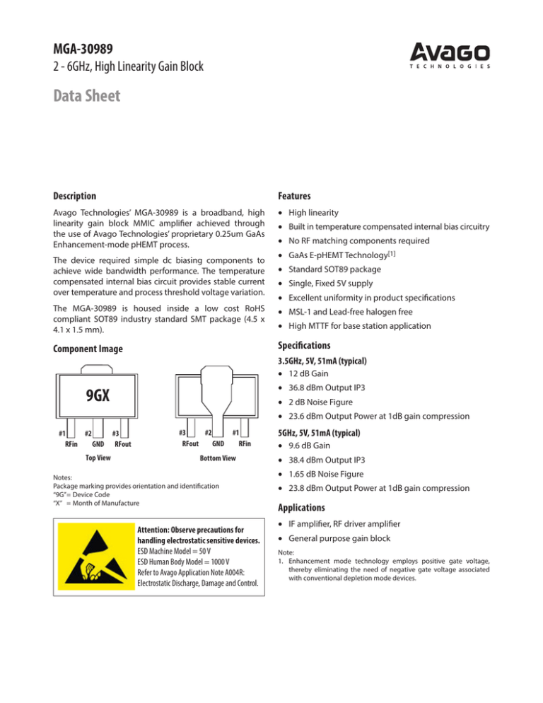
Component Image
3.5GHz, 5V, 51mA (typical)
• 12 dB Gain
• 36.8 dBm Output IP3
9GX
• 2 dB Noise Figure
• 23.6 dBm Output Power at 1dB gain compression
#1
#2
RFin
GND
Top View
#3
RFout
#3
#2
RFout
GND
#1
RFin
Bottom View
Notes:
Package marking provides orientation and identification
“9G”= Device Code
“X” =Month of Manufacture
Attention: Observe precautions for
handling electrostatic sensitive devices.
ESD Machine Model = 50 V
ESD Human Body Model = 1000 V
Refer to Avago Application Note A004R:
Electrostatic Discharge, Damage and Control.
5GHz, 5V, 51mA (typical)
• 9.6 dB Gain
• 38.4 dBm Output IP3
• 1.65 dB Noise Figure
• 23.8 dBm Output Power at 1dB gain compression
Applications
• IF amplifier, RF driver amplifier
• General purpose gain block
Note:
1. Enhancement mode technology employs positive gate voltage,
thereby eliminating the need of negative gate voltage associated
with conventional depletion mode devices.
Absolute Maximum Rating[1] TA=25°C
Thermal Resistance
Symbol
Parameter
Units
Absolute Max.
Vdd,max
Device Voltage, RF output to ground
V
5.5
Pin,max
CW RF Input Power
dBm
24
Pdiss
Total Power Dissipation [3]
W
0.47
Tj,MAX
Junction Temperature
°C
150
TSTG
Storage Temperature
°C
-65 to 150
Thermal Resistance [2] θJC = 81.2°C/W
(Vdd = 5 V, Ids = 48 mA, Tc = 85°C)
Notes:
1. Operation of this device in excess of any of
these limits may cause permanent damage.
2. Thermal resistance measured using Infrared
measurement technique.
3. This is limited by maximum Vdd and Ids.
Derate 12.3 mW/°C for Tc >112°C.
Product Consistency Distribution Charts[1, 2]
LSL
USL
50
LSL
60
USL
8.5
Figure 1. Ids, LSL=42mA , nominal=51mA, USL=66mA
9
9.5
10
10.5
Figure 2. Gain, LSL=8.5dB, nominal=9.6dB, USL=10.5dB
LSL
LSL
35
36
37
38
39
22
Figure 3. OIP3, LSL=35dBm, nominal=38.4dBm
22.5
23
23.5
24
24.5
Figure 4. P1dB, LSL=22dBm, nominal=23.8dBm
USL
Notes:
1. Distribution data sample size is 3000 samples taken from 3 different
wafer lots. Future wafers allocated to this product may have nominal
values anywhere between the upper and lower limits.
2. Measurements were made on a characterization test board, which
represents a trade-off between optimal OIP3, gain and P1dB. Circuit
trace losses have not been de-embedded from measurements
above.
1.4
1.5
1.6
1.7
1.8
Figure 5. NF, nominal=1.65dB, USL=2.1dB
2
1.9
2
2.1
Electrical Specifications [1]
TA = 25°C, Vdd = 5V
Symbol
Parameter and Test Condition
Frequency
Units
Min.
Typ.
Max.
Ids
Quiescent current
N/A
mA
42
51
66
Gain
Gain
3.5 GHz
5 GHz
dB
8.5
12
9.6
10.5
OIP3 [2]
Output Third Order Intercept Point
3.5 GHz
5 GHz
dBm
35
36.8
38.4
–
NF
Noise Figure
3.5 GHz
5 GHz
dB
–
2
1.65
2.1
S11
Input Return Loss, 50Ω source
3.5 GHz
5 GHz
dB
-18
-16
S22
Output Return Loss, 50Ω load
3.5 GHz
5 GHz
dB
-16
-15
S12
Reverse Isolation
3.5 GHz
5 GHz
dB
-21
-18
OP1dB
Output Power at 1dB Gain Compression
3.5 GHz
5 GHz
dBm
22
22
23.8
–
Notes:
1. Measurements obtained using demo board described in Figure 22 and 23. Both 3.5GHz and 5GHz data were taken with 3GHz - 6GHz Application
Test Circuits.
2. OIP3 test condition: FRF1 - FRF2 = 10MHz with input power of -10dBm per tone measured at worse side band.
3. Use proper bias, heat sink and de-rating to ensure maximum channel temperature is not exceeded. See absolute maximum ratings and application
note (if applicable) for more details.
3
Typical Performance (2GHz - 4GHz)
TA = 25°C, Vdd = 5V, Input Signal = CW. Application Test Circuit is shown in Figure 22 and Table 1.
80
60
Gain (dB)
Ids (mA)
70
50
85°C
25°C
-40°C
2.0
2.1
2.2
2.3
2.4
2.5
2.6
2.7
2.8
2.9
3.0
3.1
3.2
3.3
3.4
3.5
3.6
3.7
3.8
3.9
4.0
90
80
70
60
50
40
30
20
0
10
-10
-20
-40
30
-30
40
16
15
14
13
12
11
10
9
8
7
6
Temperature (°C)
Frequency (GHz)
Figure 7. Gain over Frequency and Temperature
P1dB(dBm)
46
44
42
40
38
36
34
32
30
28
26
27
26
25
24
23
22
21
20
19
18
17
85°C
25°C
-40°C
2.0
2.1
2.2
2.3
2.4
2.5
2.6
2.7
2.8
2.9
3.0
3.1
3.2
3.3
3.4
3.5
3.6
3.7
3.8
3.9
4.0
85°C
25°C
-40°C
2.0
2.1
2.2
2.3
2.4
2.5
2.6
2.7
2.8
2.9
3.0
3.1
3.2
3.3
3.4
3.5
3.6
3.7
3.8
3.9
4.0
OIP3 (dBm)
Figure 6. Ids over Temperature
Frequency (GHz)
Figure 8. OIP3 over Frequency and Temperature
Figure 9. P1dB over Frequency and Temperature
0
0
-5
-5
-10
-10
-15
-15
S22 (dB)
-20
-25
-30
85°C
25°C
-40°C
-35
2.0
2.1
2.2
2.3
2.4
2.5
2.6
2.7
2.8
2.9
3.0
3.1
3.2
3.3
3.4
3.5
3.6
3.7
3.8
3.9
4.0
-40
Frequency (GHz)
Figure 10. S11 over Frequency and Temperature
4
-20
-25
-30
85°C
25°C
-40°C
-35
-40
2.0
2.1
2.2
2.3
2.4
2.5
2.6
2.7
2.8
2.9
3.0
3.1
3.2
3.3
3.4
3.5
3.6
3.7
3.8
3.9
4.0
S11 (dB)
Frequency (GHz)
Frequency (GHz)
Figure 11. S22 over Frequency and Temperature
Typical Performance (2GHz - 4GHz)
TA = 25°C, Vdd = 5V, Input Signal = CW. Application Test Circuit is shown in Figure 22 and Table 1.
-16
-18
-22
NF(dB)
S12 (dB)
-20
-24
-26
85°C
25°C
-40°C
-28
85°C
25°C
-40°C
2.0
2.1
2.2
2.3
2.4
2.5
2.6
2.7
2.8
2.9
3.0
3.1
3.2
3.3
3.4
3.5
3.6
3.7
3.8
3.9
4.0
2.0
2.1
2.2
2.3
2.4
2.5
2.6
2.7
2.8
2.9
3.0
3.1
3.2
3.3
3.4
3.5
3.6
3.7
3.8
3.9
4.0
-30
5.0
4.5
4.0
3.5
3.0
2.5
2.0
1.5
1.0
0.5
0.0
Frequency (GHz)
Frequency (GHz)
Figure 12. S12 over Frequency and Temperature
Figure 13. Noise Figure over Frequency and Temperature
Typical Performance (3GHz - 6GHz)
TA = 25°C, Vdd = 5V, Input Signal = CW. Application Test Circuit is shown in Figure 22 and Table 2.
3.0
3.2
3.4
90
80
70
60
50
40
30
20
10
0
-10
-20
-40
30
-30
40
Temperature (°C)
Frequency (GHz)
Figure 16. OIP3 over Frequency and Temperature
5
5.8
6.0
5.2
5.4
5.6
4.6
4.8
5.0
4.0
4.2
4.4
Frequency (GHz)
27
26
25
24
23
22
21
20
19
18
17
85°C
25°C
-40°C
3.0
3.2
3.4
3.6
3.8
4.0
4.2
4.4
4.6
4.8
5.0
5.2
5.4
5.6
5.8
6.0
P1dB(dBm)
Figure 15. Gain over Frequency and Temperature
85°C
25°C
-40°C
3.4
3.6
3.8
3.0
3.2
OIP3 (dBm)
Figure 14. Ids over Temperature
46
44
42
40
38
36
34
32
30
28
26
5.6
5.8
6.0
50
85°C
25°C
-40°C
4.6
4.8
5.0
5.2
5.4
60
Gain (dB)
Ids (mA)
70
16
15
14
13
12
11
10
9
8
7
6
3.6
3.8
4.0
4.2
4.4
80
Frequency (GHz)
Figure 17. P1dB over Frequency and Temperature
Typical Performance (3GHz - 6GHz)
TA = 25°C, Vdd = 5V, Input Signal = CW. Application Test Circuit is shown in Figure 22 and Table 2.
0
0
85°C
25°C
-40°C
-5
-10
S22 (dB)
-15
-15
-20
-25
-25
-30
-30
3.0
3.2
3.4
3.6
3.8
4.0
4.2
4.4
4.6
4.8
5.0
5.2
5.4
5.6
5.8
6.0
-20
3.0
3.2
3.4
3.6
3.8
4.0
4.2
4.4
4.6
4.8
5.0
5.2
5.4
5.6
5.8
6.0
S11 (dB)
-10
Frequency (GHz)
Frequency (GHz)
Figure 18. S11 over Frequency and Temperature
Figure 19. S22 over Frequency and Temperature
-11
85°C
25°C
-40°C
-13
-17
-19
-21
-23
3.0
3.2
3.4
3.6
3.8
4.0
4.2
4.4
4.6
4.8
5.0
5.2
5.4
5.6
5.8
6.0
-25
Frequency (GHz)
Figure 20. S12 over Frequency and Temperature
5.0
4.5
4.0
3.5
3.0
2.5
2.0
1.5
1.0
0.5
0.0
85°C
25°C
-40°C
3.0
3.2
3.4
3.6
3.8
4.0
4.2
4.4
4.6
4.8
5.0
5.2
5.4
5.6
5.8
6.0
NF(dB)
S12 (dB)
-15
6
85°C
25°C
-40°C
-5
Frequency (GHz)
Figure 21. Noise Figure over Frequency and Temperature
Application Schematic Components Table and Demo Board
Vdd
C1
Top View
C2
C3
L1
RFin
C14
C7
RFin 1
GND 2
Vdd
RFout 3
C8
C13
RFout
Figure 22. Application Schematic
C14
C13
– Recommended PCB material is 10 mils Rogers RO4350,
with FR4 backing for mechanical strength.
– Suggested component values may vary according to
layout and PCB material.
Figure 23. Demo board Layout
7
Demo board Part List
Table 1. 2GHz - 4GHz Application Schematic Components
Circuit Symbol
Size
Value
Part Number
Description
L1
0603
8.2nH
LLQ1608-F8N2 (Toko)
Wire Wound Chip Inductor
C1
0402
100pF
GRM1555C1H101JZ01 (Murata)
Ceramic Chip Capacitor
C2
0402
0.1uF
GRM155R71C104KA88D (Murata)
Ceramic Chip Capacitor
C3
0805
2.2uF
GRM21BR61E225KA12L (Murata)
Ceramic Chip Capacitor
C7
0402
1nH
LL1005-FHL1N0 (Toko)
MLC Inductor
C8
0402
1nH
LL1005-FHL1N0 (Toko)
MLC Inductor
C13
0402
39pF
CM05CH390J50AH (Kyocera)
Ceramic Chip Capacitor
C14
0402
39pF
CM05CH390J50AH (Kyocera)
Ceramic Chip Capacitor
Table 2. 3GHz - 6GHz Application Schematic Components
Circuit Symbol
Size
Value
Part Number
Description
L1
0603
8.2nH
LLQ1608-F8N2 (Toko)
Wire Wound Chip Inductor
C1
0402
100pF
GRM1555C1H101JZ01 (Murata)
Ceramic Chip Capacitor
C2
0402
0.1uF
GRM155R71C104KA88D (Murata)
Ceramic Chip Capacitor
C3
0805
2.2uF
GRM21BR61E225KA12L (Murata)
Ceramic Chip Capacitor
C7
0402
39pF
CM05CH390J50AH (Kyocera)
Ceramic Chip Capacitor
C8
0402
39pF
CM05CH390J50AH (Kyocera)
Ceramic Chip Capacitor
C13
NA
C14
NA
Test Circuit for S-Parameter and Noise Parameter
Top View
Port1
RFin
1
GND
2
Vdd 3
RFout
Figure 24. S-parameter and Noise parameter test circuit
8
Port2 /
Bias Tee
Typical S-Parameter (Vdd = 5V, TA = 25°C, 50 ohm)
Freq (GHz)
S11
(dB)
S11
(ang)
S21
(dB)
S21
(ang)
S12
(dB)
S12
(ang)
S22
(dB)
S22
(ang)
0.1
-0.83
171.33
-49.08
107.91
-70.09
11.18
-11.42
156.15
0.5
-0.85
133.94
-29.47
73.45
-72.22
8.53
-9.79
54.38
1
-1.73
69.70
-7.88
124.85
-51.74
42.20
-7.59
-28.70
1.5
-18.64
13.90
14.19
-16.36
-28.40
-110.19
-13.30
-84.47
2
-16.77
21.81
15.26
-118.45
-24.68
162.38
-16.46
-119.30
2.2
-17.69
26.98
15.08
-146.17
-23.80
140.85
-20.71
-136.97
2.4
-17.47
27.84
14.78
-169.72
-23.09
123.10
-27.25
-147.15
2.6
-17.54
21.54
14.41
169.77
-22.45
107.84
-36.62
-119.61
2.8
-18.71
9.75
14.06
151.46
-21.86
94.47
-33.44
-73.79
3
-21.50
-7.64
13.71
134.78
-21.30
82.34
-29.50
-90.05
3.2
-26.62
-45.95
13.35
119.28
-20.77
71.05
-26.66
-116.49
3.4
-25.94
-124.50
12.98
104.86
-20.30
60.36
-23.92
-140.25
3.6
-20.44
-160.65
12.60
91.24
-19.87
50.23
-21.74
-159.02
3.8
-16.93
-177.59
12.21
78.46
-19.49
40.73
-20.32
-173.92
4
-14.77
170.22
11.82
66.38
-19.14
31.67
-19.31
175.19
4.2
-13.39
160.76
11.45
54.96
-18.81
23.05
-19.03
166.34
4.4
-12.66
151.96
11.09
43.99
-18.49
14.81
-19.23
160.06
4.6
-12.37
142.32
10.78
33.45
-18.16
6.72
-19.80
154.58
4.8
-12.28
131.95
10.50
23.16
-17.82
-1.24
-20.57
150.45
5
-12.32
119.49
10.23
12.97
-17.50
-9.24
-21.46
145.29
5.2
-11.90
102.53
9.97
2.27
-17.18
-17.80
-24.67
123.26
5.4
-11.51
86.82
9.69
-7.74
-16.90
-25.83
-23.37
106.21
5.6
-10.94
70.38
9.40
-17.72
-16.65
-33.97
-21.51
91.68
5.8
-10.14
53.71
9.10
-27.77
-16.45
-42.22
-19.44
79.92
6
-9.13
38.09
8.75
-37.67
-16.30
-50.47
-17.49
69.67
6.2
-8.04
24.75
8.37
-47.47
-16.21
-58.70
-15.67
59.26
6.4
-6.95
13.52
7.95
-57.15
-16.17
-66.81
-13.97
48.91
6.6
-5.97
4.20
7.50
-66.64
-16.19
-74.66
-12.52
38.89
6.8
-5.14
-2.97
7.00
-75.60
-16.24
-82.14
-11.26
28.93
7
-4.46
-8.67
6.51
-83.99
-16.31
-89.21
-10.27
19.35
8
-2.90
-25.68
4.58
-121.23
-16.31
-120.23
-7.84
-28.28
9
-2.46
-52.31
2.99
-158.46
-16.20
-152.20
-6.19
-69.12
10
-1.73
-90.52
0.67
164.95
-16.99
175.54
-4.64
-97.97
11
-0.89
-118.15
-2.55
136.43
-18.81
150.58
-3.14
-118.40
12
-0.61
-129.25
-5.00
117.68
-19.97
134.70
-2.55
-131.60
13
-0.76
-143.32
-6.00
96.90
-19.81
116.35
-2.38
-146.90
14
-1.01
-166.19
-6.20
70.58
-18.85
92.19
-2.68
-168.13
15
-0.88
168.37
-7.47
41.66
-19.03
65.52
-2.36
162.57
16
-0.85
157.29
-8.58
25.78
-18.91
51.09
-2.07
153.40
17
-1.18
147.97
-8.14
9.21
-17.33
35.32
-2.29
140.45
18
-1.83
133.03
-7.18
-10.20
-15.36
16.25
-2.52
133.73
19
-3.05
112.54
-5.32
-38.11
-12.58
-11.48
-4.28
116.79
20
-4.26
92.05
-4.57
-70.41
-10.96
-43.88
-5.03
93.24
9
Typical Noise Parameters (Vdd = 5V, TA = 25°C, 50 ohm)
Freq (GHz)
Fmin (dB)
Γopt Mag
Γopt Ang
Rn/Z0
2.0
2.95
0.086
49
0.52
2.5
2.32
0.12
90
0.29
3.0
1.83
0.15
122
0.19
3.5
1.54
0.18
174
0.18
4.0
1.53
0.22
-145
0.17
4.5
1.61
0.24
-103
0.21
5.0
1.78
0.27
-62
0.22
5.5
2.05
0.30
-35
0.32
6.0
2.22
0.33
-7.8
0.37
10
Part Number Ordering Information
Part Number
No. of Devices
Container
MGA-30989-BLKG
100
7” Tape/Reel
MGA-30989-TR1G
3000
13” Tape/Reel
SOT89 Package Dimensions
D
D
D1
D1
E1
POLISH
E1
OR
E
L
L
e
e
S
S
e1
C
e1
1.625
D2
MATTE FINISH
HALF ETCHING
DEPTH 0.100
1.23
2.35
0.77
0.2
D1
E
b
b1
b
POLISH
1.24
E
A
OR
b1
Dimensions in mm
Symbols
11
Minimum
Nominal
Dimensions in inches
Maximum
Minimum
Nominal
Maximum
A
1.40
1.50
1.60
0.055
0.059
0.063
L
0.89
1.04
1.20
0.0350
0.041
0.047
b
0.36
0.42
0.48
0.014
0.016
0.018
b1
0.41
0.47
0.53
0.016
0.018
0.030
0.017
C
0.38
0.40
0.43
0.014
0.015
D
4.40
4.50
4.60
0.173
0.177
0.181
D1
1.40
1.60
1.75
0.055
0.062
0.069
D2
1.45
1.65
1.80
0.055
0.062
0.069
E
3.94
-
4.25
0.155
-
0.167
E1
2.40
2.50
2.60
0.094
0.098
0.102
e1
2.90
3.00
3.10
0.114
0.118
0.122
S
0.65
0.75
0.85
0.026
0.030
0.034
e
1.40
1.50
1.60
0.054
0.059
0.063
Device Orientation
USER FEED
DIRECTION
9GX
9GX
9GX
CARRIER
TAPE
9GX
REEL
COVER TAPE
Tape Dimensions
Ø 1.5 +0.1/-0.0
8.00
0.30 ± .05
Ø 1.50 MIN.
2.00 ± .05 SEE NOTE 3
4.00 SEE NOTE 1
A
R 0.3 MAX.
1.75 ± .10
5.50 ± .05
SEE NOTE 3
Bo
12.0 ± .3
Ko
SECTION A - A
12
Ao
Ao = 4.60
Bo = 4.90
Ko = 1.90
R 0.3 TYP.
A
DIMENSIONS IN MM
NOTES:
1. 10 SPROCKET HOLE PITCH CUMULATIVE TOLERANCE ±0.2
2. CAMBER IN COMPLIANCE WITH EIA 481
3. POCKET POSITION RELATIVE TO SPROCKET HOLE MEASURED
AS TRUE POSITION OF POCKET, NOT POCKET HOLE
Reel Dimensions – 13” Reel
R
LOKREEL
R
MINNEAPOLIS USA
U.S PAT 4726534
102.0
REF
1.5
ATTENTION
Electrostatic Sensitive Devices
Safe Handling Required
88 REF
330.0
REF
"A"
96.5
6
PS
Detail "B"
6
PS
Detail "A"
8.4 - 0.2
(MEASURED AT HUB)
11.1 MAX.
Ø 20.2
Dimensions in mm
M IN
+0.5
Ø 13.0 -0.2
2.0 ± 0.5
For product information and a complete list of distributors, please go to our web site:
+0.3
(MEASURED AT HUB)
www.avagotech.com
Avago, Avago Technologies, and the A logo are trademarks of Avago Technologies in the United States and other countries.
Data subject to change. Copyright © 2005-2013 Avago Technologies. All rights reserved.
AV02-2251EN - November 11, 2013


