Datasheet - Mouser Electronics
advertisement
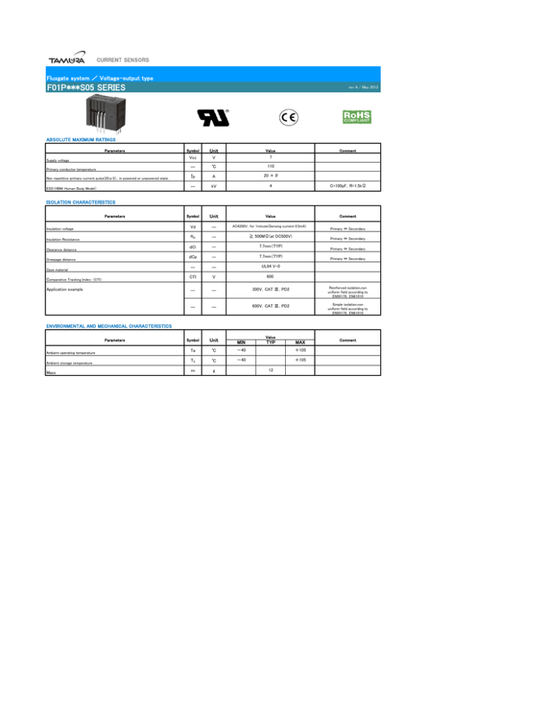
CURRENT SENSORS Fluxgate system / Voltage-output type F01P***S05 SERIES rev A / May 2013 ABSOLUTE MAXIMUM RATINGS Parameters Supply voltage Primary conductor temperature Non repetitive primary current pulse(20μS),in powered or unpowered state. ESD(HBM: Human Body Model) Symbol Unit Value Vcc V 7 ― ℃ 110 Îp A 20 × If ― kV 4 Symbol Unit Value Vd ― AC4200V,for 1minute(Sensing current 0.5mA) Comment C=100pF,R=1.5kΩ ISOLATION CHARACTERISTICS Parameters lnsulation voltage lnsulation Resistance Clearance distance Creepage distance Case material Comparative Tracking Index; (CTI) Application example RIS ― ≧ 500MΩ(at DC500V) dCi ― 7.7mm(TYP) dCp ― 7.7mm(TYP) ― ― UL94 V-0 Comment Primary ⇔ Secondary Primary ⇔ Secondary Primary ⇔ Secondary Primary ⇔ Secondary CTI V 600 ― ― 300V,CAT Ⅲ,PD2 Reinforced isolation,non uniform field according to EN50178,EN61010 ― ― 600V,CAT Ⅲ,PD2 Simple isolation,non uniform field according to EN50178,EN61010 Symbol Unit MIN Ta ℃ -40 TS ℃ -40 m g ENVIRONMENTAL AND MECHANICAL CHARACTERISTICS Parameters Ambient operating temperature Ambient storage temperature Mass Value TYP MAX +105 +105 12 Comment CURRENT SENSORS SPECIFICATIONS Ta=+25℃,RL=10kΩ,Vcc=+5V Parameters Rated Current F01P006S05 Symbol Unit If A Value MIN F01P015S05 15 F01P025S05 25 50 -20 20 F01P015S05 -51 51 F01P025S05 -85 85 F01P050S05 -150 150 F01P006S05 Supply Voltage Number of primary turns Number of secondary turns F01P006S05 Ipmax A 4.75 V Np T 1,2,3 Ns T 1816 F01P015S05 1737 F01P025S05 1764 F01P006S05 25 mA F01P015S05 30 F01P025S05 35 Output voltage Output voltage(at Ip=0A) Electrical offset current reffered to primary Temperature coefficient of Output voltage(at Ip=0A) V Vo V Voe mV 0.375 -10.40 10.40 F01P015S05 -7.10 7.10 F01P025S05 -6.25 6.25 F01P050S05 -5.80 5.80 -0.10 0.10 F01P015S05 -0.17 0.17 F01P025S05 -0.25 0.25 F01P050S05 -0.46 F01P006S05 F01P006S05 Ioe A 0.46 ±10.0 ±80.0 ppm/K of 2.5V F01P015S05 ±7.5 ±70.0 (-40℃~+105℃) F01P025S05 ±6.5 ±60.0 ±6.0 ±60.0 F01P006S05 F01P006S05 TCVo ppm/K Gth 104.2 mV/A 25 F01P050S05 12.5 Temperature coefficient of Sensitivity(at Ta=-40℃~+105℃) Output Linearity Magnetic offset current reffered to primary(at 10×If) F01P006S05 625mV/If 41.67 F01P025S05 Sensitivity error Offset voltage value is after removal of core hysteresis. 4.625 2.5 F01P015S05 Output current noise reffered to primary(at 100Hz~100kHz) Icc=15+Ip(mA)/Ns 55 Vo F01P050S05 Sensitivity(Theoretical value) 5.25 1600 Icc F01P050S05 Electrical offset voltage 5.00 Vcc F01P050S05 Consumption current (at If) Comment MAX 6 F01P050S05 Maximum current(at Vcc=+5V,Ta=+105℃) TYP εG % TCG ppm/K -0.7 0.7 ±40 εL % -0.1 IOM A -0.1 Ino μA/(Hz)1/2 0.1 0.1 36 F01P015S05 90 F01P025S05 150 F01P050S05 300 RL=1kΩ CURRENT SENSORS SPECIFICATIONS Ta=+25℃,RL=10kΩ,Vcc=+5V Parameters MAX 160 F01P015S05 15 60 F01P025S05 10 40 F01P050S05 5 Comment RL=1kΩ 20 RL=1kΩ,di/dt=18A/μs F01P015S05 0.3 RL=1kΩ,di/dt=44A/μs F01P025S05 0.3 RL=1kΩ,di/dt=68A/μs F01P050S05 0.3 RL=1kΩ,di/dt=100A/μs 0.3 RL=1kΩ,di/dt=18A/μs F01P015S05 0.3 RL=1kΩ,di/dt=44A/μs F01P025S05 0.3 RL=1kΩ,di/dt=68A/μs F01P050S05 0.3 RL=1kΩ,di/dt=100A/μs 0.6 RL=1kΩ,di/dt=If/μs Response time 2 (at 10% of If to 90% of Vo ) Frequency bandwidth(±1dB) Frequency bandwidth(±3dB) F01P006S05 Output Voltage Accuracy(Overall) MIN 0.3 F01P006S05 Response time 1 (at 90% of If ) mV 40 F01P006S05 Reaction time(at 10% of If ) Unit ― Value TYP F01P006S05 Peak to peak output ripple at oscillator freqency(f typ=450kHz) Symbol tra tr μs μs tr μs BW kHz 200 BW kHz 300 XG % RL=1kΩ RL=1kΩ XG=(100×Voe/625)+εG+εL 2.5 F01P015S05 1.9 F01P025S05 1.8 F01P050S05 1.7 STANDARDS EN50178,EN61010-1,EN60950-1,UL508(file №E243511) ※Please refer to the another sheet about conditions of UL Recognition. Ip Characteristic curve(TYP) Output Voltage Vo[V] 5 (4.625) 2.5 Primary current Ip[A] (0.375) -Ipmax (≒-If×3) -If 0 If Ipmax (≒If×3) Figure 1:Linearity curve Figure 2:Frequency response curve ex)F01P025S05 Measurement condition Ta=+25℃,RL=1kΩ,Ip=3A,Vcc=+5V CURRENT SENSORS SUPPORT DOCUMENTATION Ip(A) Ip(A) Maximum continuous DC primary current Figure 4:Ip vs Ta for F01P015S05 Ip(A) Ip(A) Figure 3:Ip vs Ta for F01P006S05 Figure 5:Ip vs Ta for F01P025S05 Figure 6:Ip vs Ta for F01P050S05 According to which the following conditions are true the maximum continuous DC primary current plot shows the boundary of the area. ①Ip < Ipmax ②Junction temperature Tj < 125℃ ③Primary conductor temperature < 110℃ ④Resistor power dissipation < 0.5 x rated power Frequency derating Figure 7:Maximum RMS AC primary current/maximum DC primary current vs frequency CURRENT SENSORS CONNECTION IN 1,2,3 13 Ip Int REF Vcc 10 9 8 If/3 OUT IN 40kΩ OUT 12 8,9,10 10kΩ OUT 10kΩ 40kΩ DIMENSIONS(mm) RECOMMENDED HOLE DIAMETER(mm) 1 2 3 10 9 8 1 2 3 10 9 8 1 2 3 If/2 + Rm GND 1Ω 10pF 11 OUT IN Vo If IN OUT Mouser Electronics Authorized Distributor Click to View Pricing, Inventory, Delivery & Lifecycle Information: Tamura: F01P015S05 F01P025S05 F01P050S05 F01P006S05
