R V dt di RC dt di τ dt di RC τ τ i τ τ i −= + + + =
advertisement
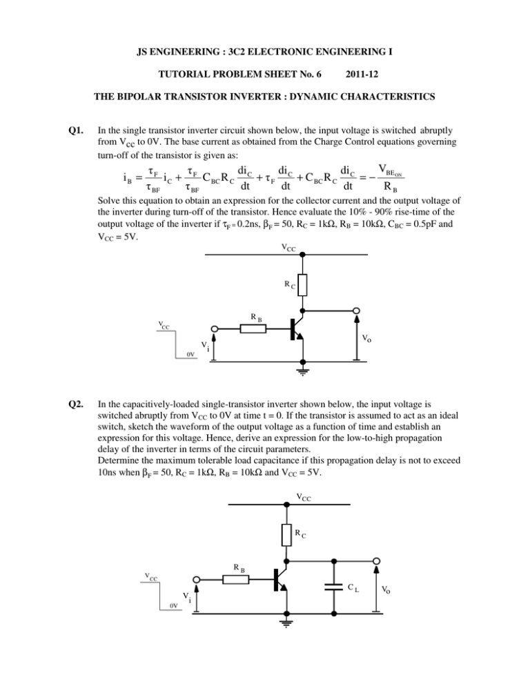
JS ENGINEERING : 3C2 ELECTRONIC ENGINEERING I TUTORIAL PROBLEM SHEET No. 6 2011-12 THE BIPOLAR TRANSISTOR INVERTER : DYNAMIC CHARACTERISTICS Q1. In the single transistor inverter circuit shown below, the input voltage is switched abruptly from Vcc to 0V. The base current as obtained from the Charge Control equations governing turn-off of the transistor is given as: iB = VBE ON di di di τF τ i C + F C BC R C C + τ F C + C BC R C C = − τ BF τ BF dt dt dt RB Solve this equation to obtain an expression for the collector current and the output voltage of the inverter during turn-off of the transistor. Hence evaluate the 10% - 90% rise-time of the output voltage of the inverter if τF = 0.2ns, βF = 50, RC = 1kΩ, RB = 10kΩ, CBC = 0.5pF and VCC = 5V. VCC RC RB V CC V 0V Q2. Vo i In the capacitively-loaded single-transistor inverter shown below, the input voltage is switched abruptly from VCC to 0V at time t = 0. If the transistor is assumed to act as an ideal switch, sketch the waveform of the output voltage as a function of time and establish an expression for this voltage. Hence, derive an expression for the low-to-high propagation delay of the inverter in terms of the circuit parameters. Determine the maximum tolerable load capacitance if this propagation delay is not to exceed 10ns when βF = 50, RC = 1kΩ, RB = 10kΩ and VCC = 5V. VCC RC V RB CC V 0V CL i Vo

