International Journal of Advanced Research in Computer Engineering & Technology (IJARCET)
Volume 3 Issue 12, December 2014
Survey on Harmonic Mitigation Techniques in
Multilevel Inverters
Namrata Shrivastava, Assistant Professor Pawan Mehta
Abstract:
Freedom of control, efficient conversion and reliability
are key factors for any utility power equipment. The
quest for achieving these goals drove the power
technology increasingly towards the use of power
electronic devices in recent decades. These devices
however introduce undesirable harmonics into the
interconnected systems, which triggers mal-operation
and reduces the lifetime of connected systems. Several
efforts have been done toward
s the mitigation of these inherent harmonics of power
electronic switching systems in the areas of control,
topology, auxiliary circuitries and system placement.
This paper presents an overview of available techniques
for harmonic minimisation and mitigation along with a
summary of currently used techniques for multilevel
inverters which is the preferred equipment for ac
systems these days due to their modularity and other
benefits suiting medium and high power applications in
most industrial and utility applications.
Index Terms—Multilevel converter, multilevel inverter, power
converters, Diode clamped Inverter, CHB MLI, SPWM, SVM,
SHE PWM, MCPWM.
I. INTRODUCTION
Power electronic equipment application and usage has
recently seen tremendous growth in industry and utility
networks. With this has grown the urge for novel power
converters having best possible reliability with least possible
cost. Multilevel inverters have emerged as one such
equipment in medium and high voltage applications. They
comprise of an array of power semiconductors and capacitor
voltage sources, the output of which generate voltages with
stepped high voltage waveforms at the output, with power
semiconductors being exposed to reduced voltages. A twolevel inverter generates an output voltage with two states
with respect to the negative terminal, while the three-level
inverter generates three voltage states, and so on. If m is the
number of steps of the phase voltage with respect to the
common terminal, then the number of steps in the line
voltages between two phases of the load and the number of
steps p in the phase voltage of a three-phase star connected
load are k=2m+1 and p=2k-1 respectively. Increasing the
number of levels in the inverter reduces the harmonic
distortion of the produced signal. Three topologies are
popular in case of multilevel inverters namely diodeclamped (neutral-clamped) [2]; capacitor-clamped (flying
capacitors) [3] and cascaded multicell inverters [1]. The
most attractive features of multilevel inverters being:
1) Low distortion and lower dv/dt
2) Very low distortion in input current.
3) Smaller common-mode (CM) voltage thus reduced
stress to motor insulations.
4) Can operate for a lower switching frequency.
ISSN: 2278 – 1323
Demands suiting medium-voltage high-power inverters has
made cascade inverter to be extensively used in high-power
medium voltage applications such as conveyors, mills,
blowers, compressors, and pumps etc. This paper presents a
comprehensive review of established and futuristic
multilevel technology along with their modulation and
control techniques.
II. INVERTER TOPOLOGIES
A. Diode-Clamped Inverter
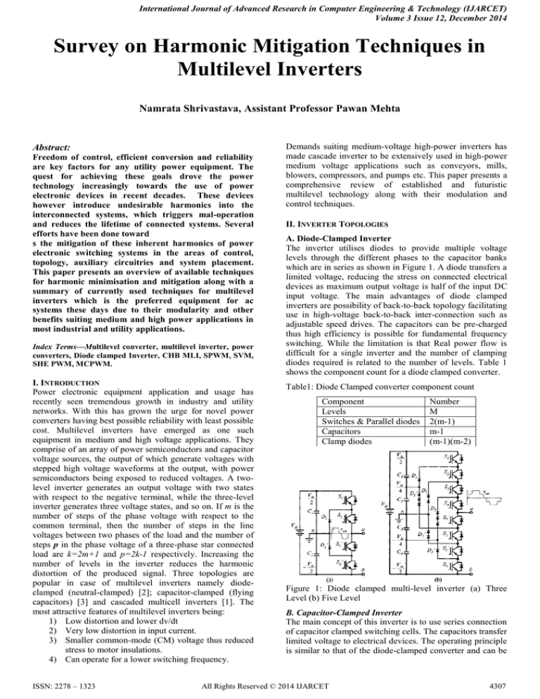
The inverter utilises diodes to provide multiple voltage
levels through the different phases to the capacitor banks
which are in series as shown in Figure 1. A diode transfers a
limited voltage, reducing the stress on connected electrical
devices as maximum output voltage is half of the input DC
input voltage. The main advantages of diode clamped
inverters are possibility of back-to-back topology facilitating
use in high-voltage back-to-back inter-connection such as
adjustable speed drives. The capacitors can be pre-charged
thus high efficiency is possible for fundamental frequency
switching. While the limitation is that Real power flow is
difficult for a single inverter and the number of clamping
diodes required is related to the number of levels. Table 1
shows the component count for a diode clamped converter.
Table1: Diode Clamped converter component count
Component
Levels
Switches & Parallel diodes
Capacitors
Clamp diodes
Number
M
2(m-1)
m-1
(m-1)(m-2)
Figure 1: Diode clamped multi-level inverter (a) Three
Level (b) Five Level
B. Capacitor-Clamped Inverter
The main concept of this inverter is to use series connection
of capacitor clamped switching cells. The capacitors transfer
limited voltage to electrical devices. The operating principle
is similar to that of the diode-clamped converter and can be
All Rights Reserved © 2014 IJARCET
4307
International Journal of Advanced Research in Computer Engineering & Technology (IJARCET)
Volume 3 Issue 12, December 2014
extended to higher numbers of output levels and clamping
diodes are not required in this type of multilevel inverters.
The major merits of this type are; huge amount of storage
capacitors provide additional ride through capabilities
during power rage, Switch combination redundancy is
provided for balancing different voltage levels and Control
of both the real and reactive power flow can be done.
While the prominent drawbacks include; a huge amount of
storage capacitors are required which makes them expensive
also the switching frequency losses are high and the
converter control gets very complicated. Table 2 shows the
component count for a diode clamped converter.
Table1: Flying capacitor converter component count
Component
Number
Levels
m
Switches & Parallel diodes 2(m-1)
Capacitors
m-1
Clamp diodes
(m-1)(m-1/2)
Soft switching can be used. While they suffer from a major
drawback as they require separate dc sources for power
conversions, a major factor that limits their application. The
number of components required for a diode clamped
converter is shown in Table 3.The power circuit for one
phase leg of a nine-level inverter with four cells in each
phase. Resulting phase voltage is synthesized by the adding
voltages generated by different cells. Each of the single
phase full bridge inverter generates three voltages at the
output: +Vdc, 0, and -Vdc. The capacitors connected to the
ac side through power switches, makes this transition
possible. The resulting output ac voltage varies from +4Vdc
to -4Vdc with nine levels, and the staircase waveform
obtained is nearly sinusoidal eliminating any requirement
for filtering.
Table3: Cascaded H-bridhe component count
Component
Number
Levels
M
Switches & Parallel diodes 2(m-1)
Clamp diodes
(m-1/2)
D. Generalized Multilevel Cells
A generalized multilevel inverter topology can be derived
from existing multilevel inverters such as diode-clamped
and capacitor clamped multilevel inverters. The generalized
multilevel inverter topology has inherent voltage level self
balancing independent of load characteristics. This
revolutionary topology provides a true multilevel structure
which can balance dc voltage level involuntarily at any
number of levels, independent of active or reactive power
conversion eliminating the requirement for any other
circuits.
Figure 2: capacitor clamped multi-level inverter (a) Three
Level (b) Five Level
C. Cascaded Multicell Inverters
The cascaded H-bride multi level inverter requires less
number of components in each level. The topology has
series of power conversion cells called an H-bridge and
gives separate input DC voltage for each H-bridge. Each cell
can provide three different voltages like zero, positive DC
and negative DC voltages.
Figure 4: P2 multilevel inverter topology
In principle, it provides a complete multilevel topology that
matches the existing multilevel inverters. Figure 6 shows the
P2 multilevel inverter structure per phase leg. Each
switching device, diode and capacitor voltage is Vdc , i.e.
1/(m-1) of the dc link voltage. An inverter with any number
of levels even the conventional two-level inverter can be
obtained using this generalized topology.
Figure 3: Cascaded multi-level inverter and its various
waveforms.
The advantages of this topology are : Has the least number
of components among all multilevel converters to obtain
same number of voltage levels, Modularized circuit
packaging is possible as each level has the same structure,
ISSN: 2278 – 1323
E. Emerging Multilevel Inverter Topologies
1) Mixed-Level Hybrid Multilevel Cells:
The multilevel diode-clamped or capacitor-clamped
inverters may be used for high-voltage high-power
applications instead of full-bridge cell in a cascaded inverter
All Rights Reserved © 2014 IJARCET
4308
International Journal of Advanced Research in Computer Engineering & Technology (IJARCET)
Volume 3 Issue 12, December 2014
to reduce the amount of separate dc sources. The nine-level
cascaded inverter shown requires four separate dc sources
for one phase leg and twelve for a three-phase inverter. If a
three-level inverter is used in place of full-bridge cell the
voltage level can be effectively doubled for each cell. Thus
to achieve the same number of levels for each phase only
two dc sources are needed per phase leg and six for a threephase inverter.
method in industrial applications is the classic sinusoidal
PWM that uses phase-shifting to eliminate the harmonics
from load voltage [4]. Another alternative is the Space
Vector strategy used in three-level inverters [6]. Low
switching frequency methods generally perform one or two
switching transition during one fundamental cycle of output
voltages to generate a staircase waveform.
Figure 7: Classification of multilevel modulation methods.
Figure 5: Mixed level hybrid diode clamped based cascaded
inverter cell using three level cells.
The configuration can be considered as mixed-level hybrid
multilevel cell structure because it has multilevel cells as the
building block of the cascaded inverter. The figure 8 shows
the nine-level cascaded inverter using three-level capacitor
clamped inverter as a cell [18]. Similarly a diode clamped
inverter can be used in place of capacitor-clamped inverter
to be a mixed-level hybrid multilevel cell.
2) Asymmetric Hybrid Multilevel Cells
Figure 8: Multicarrier phase-shifted PWM for two-cell
configuration
Figure 6: Asymmetric hybrid cascaded inverter cell
configuration
The voltage levels of the cascade inverter cells for a
cascaded multilevel inverter are equal to each other.
Different voltage levels among the cells may also be used as
are found to do so [5], the circuit thus formed is called
asymmetric hybrid multilevel inverter as in figure 6.
Depending on the availability of dc sources, this feature
allows more levels to be created in the output voltage thus
reduces the harmonic contents with lesser cell requirement
even with the same voltage level among them. Making it
possible to use high frequency PWM for one cell and lower
switching rate for other switches.
III. CONTROL AND MODULATION STRATEGIES
A. Classification of Modulation Strategies
The modulation methods used in multilevel inverters can be
classified based on switching frequency, as shown in figure7
[6]. Methods working for high switching frequencies have
multiple transitions for the static switches in one
fundamental period of output voltage. An extensively used
ISSN: 2278 – 1323
B. Multilevel SPWM
A variety of multicarrier techniques have been developed to
reduce the distortion in multilevel inverters as in classical
SPWM with triangular carriers. Some methods use carrier
disposition while others use phase shifting of multiple
carrier signals [7], [10]. A number of cascaded cells Nc in
one phase with their carriers shifted by an angle θc=360/Nc
and using the same control voltage produce a load voltage
with the smallest distortion.
C. SVM
The SVM technique can be easily extended to all multilevel
inverters [11]–[17]. The vector diagrams are universal
regardless of the type of multilevel inverter. The adjacent
three vectors can synthesize a desired voltage vector by
computing the duty cycle for each vector. Space-vector
PWM methods have the following features: optimum dclink voltage, current ripple minimisation and easier
implementation through a digital signal processor. As
number of levels increase switching states and complexity of
algorithm increases.
D. Selective Harmonic Elimination
Figure 9: Stepped voltage waveform.
A stepped voltage waveform synthesized by a (2m+1) level
inverter is shown in figure 9, where m is number of
switching angle instants. Application of Fourier analysis
provides the amplitude of odd nth harmonic of the stepped
waveform as (4) with amplitude of all even harmonics as
zero
All Rights Reserved © 2014 IJARCET
4309
International Journal of Advanced Research in Computer Engineering & Technology (IJARCET)
Volume 3 Issue 12, December 2014
4
ℎ𝑛 = 𝑛𝜋
𝑚
𝑘=1
𝑉𝑘 cos 𝑛𝛼𝑘
.............................(1)
Where Vk is the kth level of dc voltage, n is an odd
harmonic order, m is the number of switching angles and αk
is the kth switching angle. According [19] α1 to αk must
satisfy α1< α2<.....< αk<π/2. To minimize harmonic
distortion and to achieve adjustable amplitude of the
fundamental component, up to (m-1) harmonic contents can
be removed from the voltage waveform. The most
significant low-frequency harmonics are chosen for
elimination by proper selection of angles among different
level inverters. For the number of eliminated harmonics at a
constant level, all switching angles must be less than π/2.
This modulation strategy has a drawback that it provides a
narrow range of modulation index.
Figure 10: Seven-level stepped waveform half-cycle for
modulation index ranges. (a) High modulation index. (b)
Intermediate modulation index. (c) Low modulation index.
In order to achieve a wide range of modulation indexes with
minimized THD, a generalized selected harmonic
modulation scheme was proposed [8]. The method can be
illustrated by figure 10 showing the positive half-cycle of
seven-level stepped waveforms for various modulation
index levels. The range of modulation indices is hown to be
divided into three levels high, middle, and low. An output
waveform with a high modulation index level when α3 >
π/2, shown in figure 10(a) no longer exists and thus an
output waveform shown in figure 10(b) for middle
modulation index level is applied. And when the switching
angles α1 to α3dont converge at a low modulation index, the
output waveform in figure 10(c) can be used. Thus a stepped
waveform comprising of m switching angles can be divided
into m modulation index levels. With this approach low
switching frequencies with minimized harmonics in the
output waveforms can be achieved for wide range
modulation indexes.
A generalized harmonic expression for multilevel stepped
voltage has been derived [9] and is expressed as where
positive sign represents the rising edge, and the negative
sign represents a the falling edge.
4
ℎ𝑛 = 𝑛𝜋 × 𝑉1 cos 𝑛𝛼1 + 𝑉2 cos 𝑛𝛼2 ±
….±𝑉𝑚cos𝑛𝛼𝑚.........................................(2)
ISSN: 2278 – 1323
IV. FUTURE TRENDS
Multilevel inverter research and development activities are
experiencing an explosive rate of growth. Multilevel
inverters are hence becoming more and more applicable.
Based on the rapid progress of semiconductor devices and
circuit topologies, trends are rising in the following areas.
A. Applications for Distribution Voltage Level
B. Advanced High-Voltage High-Power Semiconductor
Devices
C. Use of Optical Fibers for Sensors and Controls
D. Thermal Management
E. Distributed Energy Applications
V. CONCLUSION
This paper provides a summary of multilevel inverter circuit
topologies, control strategies. The commercialization of
these circuit topologies exponentially grew since late 90’s.
Commercial products based on multilevel inverter structures
are offering attractive benefits over their counterparts and
thus research and development in the field of multilevel
inverter-related technologies is in its full swing. The
fundamental principle of most popular multilevel inverters
has been introduced systematically, various topologies along
with their relative merits and demerits is being discussed. In
addition the various novel control techniques for
optimisation of multilevel inverters have also been
introduced along with current and futuristic trends. The
present work lays a brief highlight of the evolution of
multilevel inverter technologies.
REFERENCES
[1] J. S. Lai and F. Z. Peng, “Multilevel converters–A new
breed of power converters,” IEEE Trans. Ind. Applicat., vol.
32, pp. 509–517, May/June 1996.
[2] A. Nabae, I. Takahashi, and H. Akagi, “A new neutralpoint clamped PWM inverter,” IEEE Trans. Ind. Applicat.,
vol. IA-17, pp. 518–523, Sept./Oct. 1981.
[3] T. A. Meynard and H. Foch, “Multi-level choppers for
high voltage applications,” Eur. Power Electron. Drives J.,
vol. 2, no. 1, p. 41, Mar. 1992.
[4] P. Hammond, “A new approach to enhance power
quality for medium voltage ac drives,” IEEE Trans. Ind.
Applicat., vol. 33, pp. 202–208, Jan./Feb. 1997.
[5] M. D. Manjrekar, P. K. Steimer, and T. A. Lipo,
“Hybrid multilevel power conversion system: a competitive
solution for high-power applications,” IEEE Trans. Ind.
Applicat., vol. 36, pp. 834–841, May/June 2000.
[6] N. Celanovic and D. Boroyevic, “A fast space vector
modulation algorithm for multilevel three-phase converters,”
in Conf. Rec. IEEE-IAS Annu. Meeting, Phoenix, AZ, Oct.
1999, pp. 1173–1177.
[7] L. Tolbert and T. G. Habetler, “Novel multilevel
inverter carrier-based PWM method,” IEEE Trans. Ind.
Applicat., vol. 35, pp. 1098–1107, Sept./Oct. 1999.
[39] Y. Liang and C. O. Nwankpa, “A new type of
STATCOM Based on
cascading voltage-source inverters with phase-shifted
unipolar SPWM,”
IEEE Trans. Ind. Applicat., vol. 35, pp. 1118–1123,
Sept./Oct. 1999.
[8] L. Li, D. Czarkowski, Y. Liu, and P. Pillay, “Multilevel
selective harmonic elimination PWM technique in seriesconnected voltage
inverters,” in Conf. Rec. IEEE-IAS Annu. Meeting, Oct.
1998, pp. 1454–1461.
All Rights Reserved © 2014 IJARCET
4310
International Journal of Advanced Research in Computer Engineering & Technology (IJARCET)
Volume 3 Issue 12, December 2014
[9] S. Sirisukprasert, J. S. Lai, and T. H. Liu, “Optimum
harmonic reduction with a wide range of modulation indexes
for multilevel converters,” in Conf. Rec. IEEE-IAS Annu.
Meeting, Rome, Italy, Oct. 2000, pp. 2094–2099.
[10] V. G. Agelidis and M. Calais, “Application specific
harmonic performance evaluation of multicarrier PWM
techniques,” in Proc. IEEE PESC’98, Fukuoka, Japan, May
1998, pp. 172–178.
[11] Y. H. Lee, R. Y. Kim, and D. S. Hyun, “A novel
SVPWM strategy cgyonsidering DC-link balancing for a
multi-level voltage source inverter,” in Proc. IEEE
APEC’98, 1998, pp. 509–514.
[12] B. P. McGrath, D. G. Holmes, and T. A. Lipo,
“Optimized space vector switching sequences for multilevel
inverters,” in Proc. IEEE APEC, Anaheim, CA, Mar. 4–8,
2001, pp. 1123–1129.
[13] J. Mahdavi, A. Agah, A. M. Ranjbar, and H. A. Toliyat,
“Extension of PWM space vector technique for multilevel
current-controlled voltage source inverters,” in Proc. IEEE
IECON’99, San Jose, CA, Nov. 29– Dec. 3, 1999, pp. 583–
588.
[14] L. Li, D. Czarkowski, Y. Liu, and P. Pillay, “Multilevel
space vector PWM technique based on phase-shift harmonic
suppression,” in Proc. IEEE APEC, New Orleans, LA, Feb.
2000, pp. 535–541.
[15] M. Manjrekar and G. Venkataramanan, “Advanced
topologies and modulation strategies for multilevel
inverters,” in Proc. IEEE PESC’96, Baveno, Italy, June
1996, pp. 1013–1018.
[16] D. G. Holmes and B. P. McGrath, “Opportunities for
harmonic cancellation with carrier-based PWM for twolevel and multilevel cascaded inverters,” IEEE Trans. Ind.
Applicat., vol. 37, pp. 574–582, Mar./Apr. 2001.
[17] D. W. Kang et al., “Improved carrier wave-based
SVPWM method using phase voltage redundancies for
generalized cascaded multilevel inverter topology,” in Proc.
IEEE APEC, New Orleans, LA, Feb. 2000, pp. 542–548.
[18] N. A. Rahim, M. F. M. Elias, and H. W. Ping, “A threephase five-level inverter for DTC drives application,” IEICE
Electron. Exp., vol. 8, no. 1, pp. 1–7, 2011.
[19] Gautam Poddar and Malaya Kumar Sahu, “Natural
Harmonic Elimination of Square-Wave Inverter for
Medium-Voltage Application”, IEEE Transactions On
Power Electronics, vol. 24, no. 5, may 2009, pp 1182-1188.
[20] N. Yousefpoor, S. H. Fathi, N. Farokhnia, and H. A.
Abyaneh, “THD minimization applied directly on the lineto-line voltage of multilevel inverters,” IEEE Trans. Ind.
Electron., vol. 59, no. 1, pp. 373–380, Jan. 2012.
ISSN: 2278 – 1323
AUTHOR SUMMARY
[1] Namrata Shrivastava
MTech Scholar, Technocrats Institute of Technology
Bhopal, M.P, India
[2]Assistant Professor Pawan Mehta
Technocrats College of Technology
Bhopal, M.P, India
All Rights Reserved © 2014 IJARCET
4311
