MAX78700 Datasheet - Part Number Search
advertisement
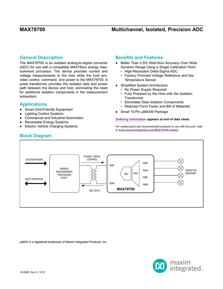
MAX78700 Multichannel, Isolated, Precision ADC General Description Benefits and Features Applications ● Simplified System Architecture • No Power Supply Required • Fully Powered by the Host with the Isolation Transformer • Eliminates Data Isolation Components • Reduced Form Factor and Bill of Materials The MAX78700 is an isolated analog-to-digital converter (ADC) for use with a compatible MAX78xxx energy measurement processor. The device provides current and voltage measurements to the host while the host provides control, command, and power to the MAX78700. A pulse transformer provides the isolated data and power path between the device and host, eliminating the need for additional isolation components in the measurement subsystem. ● ● ● ● ● ● Better Than 0.5% Watt-Hour Accuracy Over Wide Dynamic Range Using a Single Calibration Point • High-Resolution Delta-Sigma ADC • Factory-Trimmed Voltage Reference and Die Temperature Sensor Smart Grid-Friendly Equipment Lighting Control Systems Commercial and Industrial Automation Renewable Energy Systems Electric Vehicle Charging Systems ● Small 10-Pin μMAX® Package Ordering Information appears at end of data sheet. For related parts and recommended products to use with this part, refer to www.maximintegrated.com/MAX78700.related. Block Diagram POWER, TIMING, CONTROL SYSTEM POWER HOST INTERFACE INAP ISOP ENERGY MEASUREMENT PROCESSOR “HOST” ADC MUX ISON ADC DATA µMAX is a registered trademark of Maxim Integrated Products, Inc. 19-6565; Rev 0; 12/12 INAN INBP INBN MAX78700 RESISTIVE SENSORS MAX78700 Multichannel, Isolated, Precision ADC Absolute Maximum Ratings (All voltages with respect to GND.) Voltage Range INAN, INAP, INBP, INBN..............-0.5V to +4.6V Voltage Range ISOP, ISON...................................-0.5V to +4.6V Operating Temperature Range............................ -40°C to +85°C Operating Junction Temperature (Peak).......................... +140°C Operating Junction Temperature (Peak, 100ms)............. +140°C Operating Junction Temperature (Continuous)................ +125°C Storage Temperature......................................... -45°C to +165°C Lead Temperature (soldering, 10s).................................. +300°C Soldering Temperature (reflow)........................................+260°C Stresses beyond those listed under “Absolute Maximum Ratings” may cause permanent damage to the device. These are stress ratings only, and functional operation of the device at these or any other conditions beyond those indicated in the operational sections of the specifications is not implied. Exposure to absolute maximum rating conditions for extended periods may affect device reliability. Recommended External Components NAME FROM TO C1 VCC GND FUNCTION Bypass capacitor for supply VALUE UNIT 0.5 µF Performance Specifications (Limits are 100% production tested at TA = +22°C. Limits over the operating temperature range and relevant supply voltage range are guaranteed by design and characterization.) PARAMETER SYMBOL CONDITIONS Usable Input Range VIN INAP, INAN, INBP, INBN Total Harmonic Distortion THD First 10 harmonics, fIN = 65Hz, VIN = 20mV, 64kpts FFT, Blackman-Harris window Input Impedance fIN = 65Hz Temperature Coefficient of Input Impedance fIN = 65Hz (Note 1) ADC Gain Error vs. % Power-Supply Variation Input Offset MIN TYP VCC 250 MAX UNITS VCC + 250 mV peak -85 20 106 ∆NoutPK 357nV / VIN 100 ∆VCC / 3.3 dB 90 kΩ 1.7 Ω/°C 50 ppm/% VIN = 200mVP-P, 65Hz, VCC = 3.0V, 3.6V -10 +10 mV Note 1: Guaranteed by design, not subject to test. www.maximintegrated.com Maxim Integrated │ 2 MAX78700 Multichannel, Isolated, Precision ADC Pin Configuration TOP VIEW INBN 1 INBP 2 TESTENB 3 ISON ISOP + MAX78700 10 INAN 9 INAP 8 GND 4 7 VCC 5 6 TMUX µMAX Pin Description PIN NAME FUNCTION 1 INBN Channel B ADC Negative Input 2 INBP Channel B ADC Positive Input 3 TESTENB 4 ISON Transformer Negative 5 ISOP Transformer Positive 6 TMUX Host-Controlled DIO 7 VCC Output of the Rectifier Block 8 GND Ground. The 0.5µF capacitor from VCC to GND must be connected to this pin. 9 INAP Channel A ADC Positive Input 10 INAN Channel A ADC Negative Input www.maximintegrated.com Enables the Test Modes. Must be grounded in normal operation. Maxim Integrated │ 3 MAX78700 Multichannel, Isolated, Precision ADC Detailed Description ISO_INT Rectifier INBN The active rectifier in the device rectifies the power pulses received from the host through the isolation transformer to create the VCC voltage. A 2.5V regulator block powers all the digital blocks of the chip except the PLL and ISO_INT, which are powered by VCC. The PLL locks to the incoming power pulses to create reference clocks for the ADC and communications interface to the host. ADC Maxim Integrated’s proven delta-sigma ADC digitizes the voltage and current-sense voltages. Bandgap The device includes an on-chip precision bandgap voltage reference that incorporates auto-zero techniques as well as production trims to minimize errors caused by component mismatch and drift. The result is a voltage output with a predictable temperature coefficient that is compensated in firmware by the host. MAX78700 TEMP SENSE PLL INAP Figure 1 shows a block diagram of the device with a brief description of various functional blocks. PLL INAN The device continuously sends ADC data to the host. The host can request the device to return certain ancillary data such as trim information and die temperature data. The MAX78700 communicates with the host through a pulse transformer to provide isolation from the high-voltage power domain. The isolated interface block receives the incoming data from the host and transmits data back to the host through the isolation transformer. INBP The MAX78700 is an isolated current and voltage analog-to-digital converter (ADC) that is compatible with MAX78xxx hosts. The device digitizes low-level signals from shunt resistor type current sensors and resistive divider voltage measurements. MUX CLOCK GEN IBIAS GEN 2.5V REG VREF VBIAS GEN ADC 2.5V RECTIFIER VCC ISO_INT MUX CONTROL INTERFACE + MODE CONTROL TRIM OTP TMUX TESTENB ISON ISOP GND FIR Figure 1. Functional Diagram www.maximintegrated.com Maxim Integrated │ 4 MAX78700 Temperature and Power-Supply Voltage Measurement The device includes an on-chip temperature sensor. The voltage from this sensor is measured by the ADC and sent to the host. During manufacturing test, the circuit is calibrated by measuring the voltage at room temperature and storing the value in the OTP memory. A resistor-divider scales the rectified power-supply voltage, VCC, to match the input range of the ADC. The ADC measures the scaled voltage and the value is sent to the host. www.maximintegrated.com Multichannel, Isolated, Precision ADC Ordering Information PART TEMP RANGE PIN-PACKAGE MAX78700+A00 -40°C to +85°C 10 µMAX MAX78700+A00T -40°C to +85°C 10 µMAX +Denotes a lead(Pb)-free/RoHS-compliant package. T = Tape and reel. Package Information For the latest package outline information and land patterns (footprints), go to www.maximintegrated.com/packages. Note that a “+”, “#”, or “-” in the package code indicates RoHS status only. Package drawings may show a different suffix character, but the drawing pertains to the package regardless of RoHS status. PACKAGE TYPE PACKAGE CODE OUTLINE NO. LAND PATTERN NO. 10 µMAX U10+2 21-0061 90-0330 Maxim Integrated │ 5 MAX78700 Multichannel, Isolated, Precision ADC Revision History REVISION NUMBER REVISION DATE 0 12/12 DESCRIPTION Initial release PAGES CHANGED — For pricing, delivery, and ordering information, please contact Maxim Direct at 1-888-629-4642, or visit Maxim Integrated’s website at www.maximintegrated.com. Maxim Integrated cannot assume responsibility for use of any circuitry other than circuitry entirely embodied in a Maxim Integrated product. No circuit patent licenses are implied. Maxim Integrated reserves the right to change the circuitry and specifications without notice at any time. The parametric values (min and max limits) shown in the Electrical Characteristics table are guaranteed. Other parametric values quoted in this data sheet are provided for guidance. Maxim Integrated and the Maxim Integrated logo are trademarks of Maxim Integrated Products, Inc. © 2012 Maxim Integrated Products, Inc. │ 6

