Circuit Note
CN-0147
Devices Connected/Referenced
Circuit Designs Using Analog Devices Products
Apply these product pairings quickly and with confidence.
For more information and/or support call 1-800-AnalogD
(1-800-262-5643) or visit www.analog.com/circuit.
ADF4350
Fractional-N PLL IC with Integrated VCO
ADP150
Low Noise 3.3 V LDO
Powering the ADF4350 PLL and VCO with ADP150 Low Noise
LDO Regulators for Reduced Phase Noise
CIRCUIT FUNCTION AND BENEFITS
The lower integrated rms noise of the ADP150 LDO of only
9 µV rms (10 Hz to 100 kHz) helps to minimize VCO phase
noise and reduce the impact of VCO pushing (the VCO
equivalent of power supply rejection).
This circuit uses low noise, low dropout (LDO) linear regulators
to supply power to a wideband integrated PLL and VCO.
Wideband voltage controlled oscillators (VCOs) may have
increased sensitivity to power supply noise, hence, ultralow
noise regulators are recommended for best performance.
Figure 2 shows a photo of the evaluation board, which uses the
ADP150 LDOs to power the ADF4350. The ADP150 represents
the industry’s lowest noise LDO in the smallest package at the
lowest cost. It is available in a 4-ball, 0.8 mm × 0.8 mm, 0.4 mm
pitch WLCSP or a convenient 5-lead TSOT package. Adding the
ADP150’s to the design, therefore, has minimal impact on
system cost and board area while providing a significant
improvement in phase noise.
VVCO
16
CIN
1µF
ON
1
VIN
2
GND
3
EN
OFF
VOUT 5
ADP150
COUT
1µF
CIN
1µF
ON
OFF
1
VIN
2
GND
3
EN
FREF IN
28
10
DVDD AVDD
30
26
25
4
6
32
CE PDB RF VP SDV DD MUXOUT LD
1nF 1nF
29 REF IN
51Ω
RFOUTB+ 14
RFOUTB– 15
1 CLK
2 DATA
NC 4
NC = NO CONNECT
VIN = 6.0V
17
VVCO
VOUT = 3.3V
VOUT 5
ADP150
NC 4
VOUT = 3.3V
COUT
1µF
SPI-COMPATIBLE SERIAL BUS
VIN = 6.0V
LOCK
DETECT
VDD
3.9nH
3 LE
RFOUTA+ 12
22 RSET
RFOUTA– 13
4.7kΩ
1nF
VTUNE 20
680Ω
CPOUT 7
SW 5
CPGND SDGND AGND AGNDVCO
8
3.9nH
1nF
ADF4350
NC = NO CONNECT
VVCO
31
9
11 18
DGND
21
27
10pF
2700pF
TEMP VCOM VREF
19
23
0.1µF 10pF
39nF
1200pF
360Ω
24
0.1µF 10pF
0.1µF
08876-001
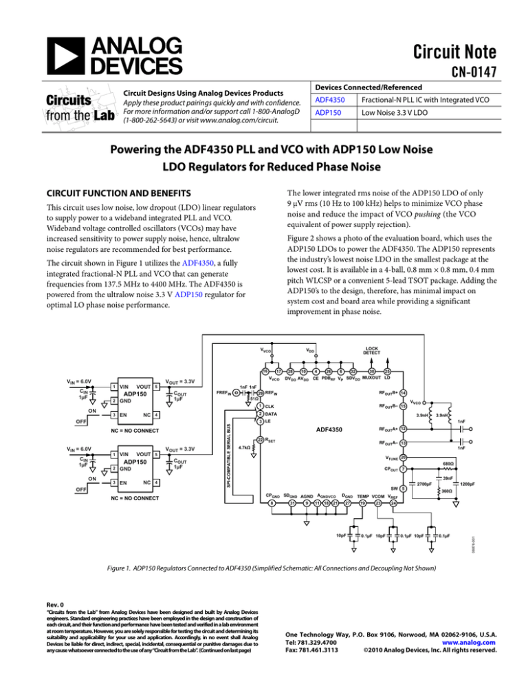
The circuit shown in Figure 1 utilizes the ADF4350, a fully
integrated fractional-N PLL and VCO that can generate
frequencies from 137.5 MHz to 4400 MHz. The ADF4350 is
powered from the ultralow noise 3.3 V ADP150 regulator for
optimal LO phase noise performance.
Figure 1. ADP150 Regulators Connected to ADF4350 (Simplified Schematic: All Connections and Decoupling Not Shown)
Rev. 0
“Circuits from the Lab” from Analog Devices have been designed and built by Analog Devices
engineers. Standard engineering practices have been employed in the design and construction of
each circuit, and their function and performance have been tested and verified in a lab environment
at room temperature. However, you are solely responsible for testing the circuit and determining its
suitability and applicability for your use and application. Accordingly, in no event shall Analog
Devices be liable for direct, indirect, special, incidental, consequential or punitive damages due to
any cause whatsoever connected to the use of any“Circuit from the Lab”. (Continued on last page)
One Technology Way, P.O. Box 9106, Norwood, MA 02062-9106, U.S.A.
Tel: 781.329.4700
www.analog.com
Fax: 781.461.3113
©2010 Analog Devices, Inc. All rights reserved.
CN-0147
Circuit Note
POWER SUPPLY
SPECTRUM ANALYZER
[R&S FSUP 26]
6.0V
EVAL-ADF4350
REV B BOARD
RF OUT
PC
08876-003
USB
CABLE
08876-002
Figure 3. ADF4350 Measurement Setup
Figure 2. EVAL-ADF4350EB1Z Rev. B Evaluation Board
Featuring ADP150 Low Noise Regulators
CIRCUIT DESCRIPTION
The ADF4350 is a wideband PLL and VCO consisting of
three separate multiband VCOs. Each VCO covers a range of
approximately 700 MHz (with some overlap between VCOs).
Lower frequencies are generated by output dividers.
VCO pushing is measured by applying a steady dc tuning voltage
to the ADF4350 VTUNE pin, varying the power supply voltage,
and measuring the frequency change. The pushing figure (P)
equals the frequency delta divided by the voltage delta, as shown
in Table 1.
In a PLL system, higher VCO pushing means that power supply
noise will degrade the VCO phase noise. If VCO pushing is low,
then power supply noise will not significantly degrade phase
noise. However, for high VCO pushing, noisy power supplies
will have a measurable impact on phase noise performance.
Table 1. ADF4350 VCO Pushing
VCO Frequency (MHz)
2200
3300
4400
VTUNE (V)
2.5
2.5
2.5
VCO Pushing (MHz/V)
0.73
1.79
5.99
Experiments showed pushing to be at its maximum at
4.4 GHz VCO output frequency, so the comparison of
VCO performance with different regulators was made at this
frequency. Rev. A evaluation boards of the ADF4350 used the
ADP3334 LDO regulator. The integrated rms noise of this
regulator is 27 µV (integrated from 10 Hz to 100 kHz). This
compares to 9 µV for the ADP150, which is used on the
EVAL-ADF4350EB1Z, Rev B. In order to measure the impact
of the power supply noise, a narrow PLL loop bandwidth (10
kHz) was used to facilitate greater examination of VCO phase
noise. A diagram of this setup is shown in Figure 3.
A more detailed examination of the output noise density with
frequency is available from the data sheets of both the ADP3334
and ADP150.
Figure 4 shows that the noise spectral density of the ADP3334
regulator is 25 nV/√Hz at 100 kHz offset. The same plot for the
ADP150 (Figure 5) shows 100 nV/√Hz.
The formula for calculating the degradation in phase noise due
to the power supply noise is as follows:
P × Sfm
L(LDO) = 20 log
2 × fm
Where L(LDO) is the noise contribution from the regulator to the
VCO phase noise (in dBc/Hz), at an offset fm; P is the VCO
pushing figure in Hz/V; Sfm is the noise spectral density at a
given frequency offset in V/√Hz; and fm is the frequency offset
at which the noise spectral density is measured in Hz.
Rev. 0 | Page 2 of 4
CN-0147
100
Table 2. Calculation and Measurement of VCO Noise
VOUT = 2.2V
IL = 1mA
10
CL = 10µF
CNR = 10nF
1
CL = 10µF
CNR = 0
Noise contribution from regulator
(nV/√Hz)
Noise contribution from regulator
(dBc/Hz)
Total calculated noise at VCO output
(dBc/Hz)
Measured VCO noise at 100 kHz offset
(dBc/Hz)
CL = 1µF
CNR = 0
0.1
CL = 1µF
CNR = 10nF
ADP3334
ADP150
150
25
−104
−119.5
−103
−109.5
−102.6
−108.5
0.01
0.001
10
100
1k
10k
100k
1M
FREQUENCY (Hz)
08876-004
VOLTAGE NOISE SPECTRAL DENSITY (µV/ Hz)
Circuit Note
Figure 4. ADP3334 Output Noise Spectrum
0.501
VOUT = 1.8V
VOUT = 2.8V
VOUT = 3.3V
0.451
0.401
NOISE (µV/ Hz)
0.351
0.301
0.251
0.201
0.151
08876-006
0.101
0.001
10
100
1k
10k
100k
FREQUENCY (Hz)
08876-005
0.051
Figure 6. ADF4350 Phase Noise at 4.4 GHz with ADP3334 Regulators
Figure 5. ADP150 output noise spectrum
The noise contribution from the supply is then rss summed
with the noise contribution of the VCO (itself measured with a
very low noise supply) to give the total noise at the VCO output
with a given regulator.
These noise performances are rss summed together to give the
expected VCO phase noise:
L(TOTAL) = L(VCO)2 + L(LDO)2
Or expressed in dB
[(
L(TOTAL) = 10 log 10LVCO / 20
) + (10
2
) ]
LLDO / 20 2
08876-007
In this example, a 100 kHz noise spectral density offset is
chosen, a 6 MHz/V pushing figure is used, and −110 dBc/Hz is
taken as the VCO noise with an ideal supply.
Figure 7. ADF4350 Phase Noise at 4.4 GHz with ADP150 Regulators
Rev. 0 | Page 3 of 4
CN-0147
Circuit Note
Using a dedicated signal source analyzer (like Rohde & Schwarz
FSUP), the VCO phase noise is compared. At 100 kHz offset the
ADP3334 delivers −102.6 dBc/Hz (Figure 6), and in the same
configuration the ADP150 measures −108.5 dBc/Hz (Figure 7).
The integrated phase noise improves from 1.95° to 1.4° rms
also. The measured results correlate very closely with the
calculations and clearly show the benefit of using the ADP150
with the ADF4350.
LEARN MORE
COMMON VARIATIONS
ADF4350 Data Sheet
Additional regulators can be added for greater isolation
between power supplies, if desired. Also, one ADF150
regulator can be used to power the entire ADF4350 part.
However, care needs to be taken in this case to ensure the
maximum rated current of the single ADP150 regulator is not
exceeded. This is possible if the lowest output power setting
on the ADF4350 is selected.
ADIsimPLL Design Tool
ADIsimPower Design Tool
Basso, C., C. Fourtet, and P. Kadanka. “Get the Best from Your
Low-Dropout Regulator.” EDN, 18 Feb. 1999.
Data Sheets and Evaluation Boards
ADF4350 Evaluation Board
ADP150 Data Sheet
ADP3334 Data Sheet
REVISION HISTORY
4/10—Revision 0: Initial Version
(Continued from first page) "Circuits from the Lab" are intended only for use with Analog Devices products and are the intellectual property of Analog Devices or its licensors. While you may
use the "Circuits from the Lab" in the design of your product, no other license is granted by implication or otherwise under any patents or other intellectual property by application or use of
the "Circuits from the Lab". Information furnished by Analog Devices is believed to be accurate and reliable. However, "Circuits from the Lab" are supplied "as is" and without warranties of any
kind, express, implied, or statutory including, but not limited to, any implied warranty of merchantability, noninfringement or fitness for a particular purpose and no responsibility is assumed
by Analog Devices for their use, nor for any infringements of patents or other rights of third parties that may result from their use. Analog Devices reserves the right to change any "Circuits
from the Lab" at any time without notice, but is under no obligation to do so. Trademarks and registered trademarks are the property of their respective owners.
©2010 Analog Devices, Inc. All rights reserved. Trademarks and
registered trademarks are the property of their respective owners.
CN08876-0-4/10(0)
Rev. 0 | Page 4 of 4


