VOL. 10, NO. 9, MAY 2015
ARPN Journal of Engineering and Applied Sciences
ISSN 1819-6608
©2006-2015 Asian Research Publishing Network (ARPN). All rights reserved.
www.arpnjournals.com
PV MICROINVERTER TOPOLOGY USING SOFT SWITCHING HALFWAVE CYCLOCONVERTER
S. Divya1, K. Abarna1 and M. Sasikumar2
1Power
Electronics and Drives, Jeppiaar Engineering College, Chennai, India
Department of Electrical and Electronics Engineering, Jeppiaar Engineering College, Chennai, India
E-Mail: judediv6@gmail.com
2
ABSTRACT
This paper deals with the development of a micro inverter for single phase photovoltaic applications which is
suitable for conversion from low voltage DC to high voltage AC. The circuit topology is based on half-wave
cycloconverter and grid connected micro inverter with a very less number of conversion stages and passive components.
To interface the full bridge converter to the half-wave cycloconverter a high- frequency transformer and series-resonant
tank are used. To determine the average output power of the inverter, a steady state analysis is used and to control the
output power of the inverter, phase-shift power modulation is used. The operational characteristic is analyzed and
multidimensional control technique is used to achieve high efficiency voltage gain, quality factor and phase shift of the
inverter. The micro inverter and converter have light weight and reduced switch count. The operation of proposed micro
inverter in grid-connected mode is validated using MATLAB simulation.
Keywords: half-wave cycloconverter, full-bridge inverter, photovoltaic (PV), high frequency transformer, series-resonant tank.
1.
INTRODUCTION
In renewable energy research centre solar energy
plays a vital role as a sustainable and low environment
impact energy source [5]. A photovoltaic (PV) system
plays a major role and set to grow fast among all potential
solar power generation systems. In grid connected PV
energy systems PV inverter is a key element. To convert
PV-generated dc power into grid synchronized ac output,
inverter plays a main function [2]. And to increase
efficiency we consider more techniques among all softswitching is choose to increase efficiency of inverter
because it reduces the loss of switching of semiconductor
devices [6]. Zero voltage switching (ZVS) is used, to set
the device when it is instantaneously blocking close to
zero volts. To simulate and implement half-wave
cycloconverter: the number of power switches should be
reduced which result in reduced switching and conduction
losses, resonant tank is used to implement soft-switching
at the turn on of the power switches to reduce switching
losses due to the increased switching frequency, to reduce
the conversion stages, and to reduce energy storage
capacitance value [3].
2.
CONVENTIONAL DC/AC POWER
CONVERTER
A. Circuit description
The full-bridge inverter is used as the primary
side inverter of the micro inverter due to its higher voltage
gain compared to the half bridge inverter, although the
number of switches in the full bridge circuit is twice that
of the half-bridge [9]. The turns ratio of the high frequency
transformer can be reduced by half, and hence, the size of
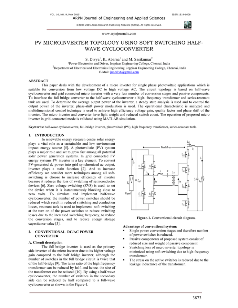
the transformer can be reduced [10]. By using a half-wave
cycloconverter, the number of switches in the secondary
side can be reduced by half compared to a full-wave
cycloconverter as shown in the Figure-1.
Figure-1. Conventional circuit diagram.
Advantage of conventional system:
Single power conversion stages and therefore number
of power switches is reduced.
Passive components of proposed system consist of
reduced size and weight of passive component.
Switching loss of micro inverter topology is
minimized using soft-switching due to high-frequency
transformer.
The stress on the active switches is reduced due to the
leakage inductance of the transformer.
3873
VOL. 10, NO. 9, MAY 2015
ARPN Journal of Engineering and Applied Sciences
ISSN 1819-6608
©2006-2015 Asian Research Publishing Network (ARPN). All rights reserved.
www.arpnjournals.com
3.
PROPOSED BOOST INVERTER SYSTEM
Mode 2 – ZCS condition
Figure-2. Proposed circuit diagram.
A proposed new two inductor,two switch boost
inverter topology that can achieve output voltage
regulation from full load to no load in a wide input voltage
range using constant frequency control.This topology
employs transformer with a unity turns ratio to couple the
current path of the two boost inductor so that the both
inductors conductidentical currentS. Due to this current
mirror effect of the transformer no energy is stored in the
inductors where there is no overlapping of conduction
time of two switches i.e. when D=0. This transformer
approach can be applied to isolated or non-isolated two
inductor, two switch topologies with any type of output
rectifier.The input side of the circuit consist of two
switches Q1 & Q2,two boost inductor L11& L12,transformer
TR.
4.
Figure-4. Circuit diagram of mode 2 operation.
During this mode of conduction the switch Q2
conduct and inductor L12 is charging,thus the current
flows in the primary side of the transformer induces
current in the secondary tapings.And U3H1 and U3L are
also turned ON.In this mode the resonant current leads the
cycloconverter input voltage vofb then ZCS occurs in the
half-wave cycloconverter.
Mode 3 – Negative
During the negative mode of operation the switch
switch Q1 Conducts and inductor L12 is charging, thus the
current flow in the primary of the transformer induces
current in the secondary tapings. And U3L1 and U3H1 are
also turned ON and produces negative half cycle.
MODES OF OPERATION
Mode 1 – Positive
During the positive mode of conduction,the
switch Q1 starts conducting and inductor L11 get
charged.Thus the current flows in the primary side
Figure-5. Circuit diagram of mode 3 operation.
5.
Figure-3. Circuit diagram of mode 1 operation.
of the transformer induces the current in the secondary
taping.And U3H1 and U3L1 are also turned ON and
produces positive half-cycle.
CIRCUIT TOPOLOGY DESCRIPTION
a) Topology description and switching sequence of
cycloconverter
The proposed micro inverter consists of fullbridge inverter which is used as the primary side of the
circuit. The high-frequency transformer is used to reduce
the turn’s ratio by half and the transformer size is also
reduced. To integrate the micro inverter to the grid at the
secondary side, a half-wave cyclo converter is used.
Therefore this may results in reduced switching and
conduction losses in the overall inverter. To eliminate the
switching frequency ripple in the output current, the output
filters capacitor and inductor in secondary side.
3874
VOL. 10, NO. 9, MAY 2015
ARPN Journal of Engineering and Applied Sciences
ISSN 1819-6608
©2006-2015 Asian Research Publishing Network (ARPN). All rights reserved.
www.arpnjournals.com
Switching sequence of cycloconverter consist of
grid voltage and PV input voltage are constant among only
one switching period of the micro inverter
6.
SIMULATION RESULTS AND DISCUSSION
Table-1. Cyclo converter switching sequences.
b) Parameters of micro inverter
Table-2. Micro inverter parameters.
Parameters
Value
Unit
Resonant capacitor
120.9
nF
Resonant inductor
84.6
µF
Input voltage
40
V
Transformer turns ratio
8
Quality factor
4
Switching frequency
42.2
Hz
RMS output voltage
230
V
Figure-7. Simulation diagram of proposed system.
Figure-8. Simulated waveform of Input voltages of a
Proposed Half-wave cycloconverter.
The input voltage of both conventional and
proposed half wave cycloconverter is given as 40V as
shown in the figure.
Figure-6. Input power and output power during MPPT
test.
Solar array simulator is used to test the capability
of maximum power point tracking in micro inverter.
Power level and voltage level of micro inverter is
measured as shown in the figure 6.Therefore MPP is
tracked more than 95% accuracy using MPPT. And to
restrict the variation of Q the resonant components L and
C should be selected appropriately. And the total
impedance of cyclo converter is given as,
Figure-9. Simulated waveform of output voltage and
current of conventional system.
Z= (2/3.14Vout)/Ires.
And, M=Vout/nVin
Where M is the instantaneous voltage gain of the inverter.
Figure-10. Simulated waveform of inductor current.
3875
VOL. 10, NO. 9, MAY 2015
ARPN Journal of Engineering and Applied Sciences
ISSN 1819-6608
©2006-2015 Asian Research Publishing Network (ARPN). All rights reserved.
www.arpnjournals.com
Thus from the above figure we come to a
conclusion that the output power of both the conventional
and proposed system are seen to be same which is greater
than 250 V even the number of switches are reduced in the
proposed system.
7.
Figure-11. Output voltage of a proposed Half-wave
cycloconverter based photovoltaic micro inverter.
The output voltage obtained here is in the level of
200 V which is said to be same voltage obtained in the
conventional system.
CONCLUSIONS
A micro inverter topology is proposed with a
half-wave cyclo converter and a two inductor with two
switches. A relationship between the inverter phase shift,
the full-bridge phase shift, the voltage gain of the inverter,
the quality factor of the series-resonant tank, and the
delivered power is derived. The soft-switching operation
of the full-bridge and the half-wave cyclo converter is
analyzed using the derived resonant current equation for
the three stepped full-bridge output voltage and the halfwave cyclo converter input voltage. Simulation results are
presented to verify the design process and the operation of
the inverter. In future the number of power switches can
be reduced which results in reduced switching and
conduction losses.
REFERENCES
[1] H. Hu, W. Al-hoor, N. H. Kutkut, I. Batarseh and Z. J.
Shen. 2010. “Efficiency improvement of grid-tied
inverters at low input power using pulse-skipping
control strategy, IEEE transaction. Power Electron,
Vol. 25, No.12, pp.3129-3138, December.
Figure-12. Output Current of a proposed Half-wave
cycloconverter based photovoltaic micro inverter.
[2] L. Zhang, K. Sun, Y. Xing, L. Feng and H. Ge. 2011.
“A modular grid connected photovoltaic generation
system based on DC bus,” IEEE Trans. Power
Electron. Vol.26, No.2, pp.523-531, February.
[3] R. Teodorescu, M. Liserre and P. Rodriquez. 2010.
“Grid converters for PV and wind power system”
New York: Wiley.
[4] X. Li and A. Bhat. 2010. “Analysis and design of
high-frequency isolated dual-bridge series resonant
DC/DC converter,” IEEE Trans. Power Electron.
Vol.25, No.4, pp.850-862, April.
Figure-13. Output power of proposed circuit.
And the above simulation of output power is
based photovoltaic based microinverter with R load.
[5] A. Hayman. 2010. “Development of a high-efficiency
solar micro-inverter,” M. S. thesis, Massachusetts
Inst. Technol., Cambridge, UK.
[6] Vasantharaj S, Vinodhkumar G, Sasikumar M. 2012.
“Development of a Fuzzy Logic based, Photovoltaic
Maximum Power Point tracking control system using
boost converter”, Proc. IET Sustainable Energy and
Intelligent Systems (SEISCON), Conf., pp. 1-6.
Figure-14. Output power of conventional system.
[7] Vasantharaj S, Sasikumar.M. 2012. “An artificial
intelligent controller for a Three Phase Inverter based
Solar PV system using boost converter”, Proc. IEEE
Advanced Computing (ICoAC 2012) Conf. pp. 1-7.
3876
VOL. 10, NO. 9, MAY 2015
ARPN Journal of Engineering and Applied Sciences
ISSN 1819-6608
©2006-2015 Asian Research Publishing Network (ARPN). All rights reserved.
www.arpnjournals.com
[8] Sasikumar M. and Pandianb S. C. 2012. “Modified bidirectional AC/DC power converter with power factor
correction”, International Journal of Engineering,
Transactions B: Applications, Vol. 25, No.3, 175-180.
[9] D. Cao, S. Jiang, and X. Yu. 2011. titled “Low-cost
semi-z-source inverter for single-phase,” IEEE Trans.
Power Electron., Vol.26, No.4, pp.3514-3523,
December.
[10] P. Krein and B. Balog, “Minimum energy and
capacitance requirements for single-phase inverters
and rectifiers using a ripple port,” IEEE Trans Power
Electron., Vol.27, No.11, pp.4690-4698.
3877
