Novel Static Differential ultra Low-Voltage and High Speed
advertisement
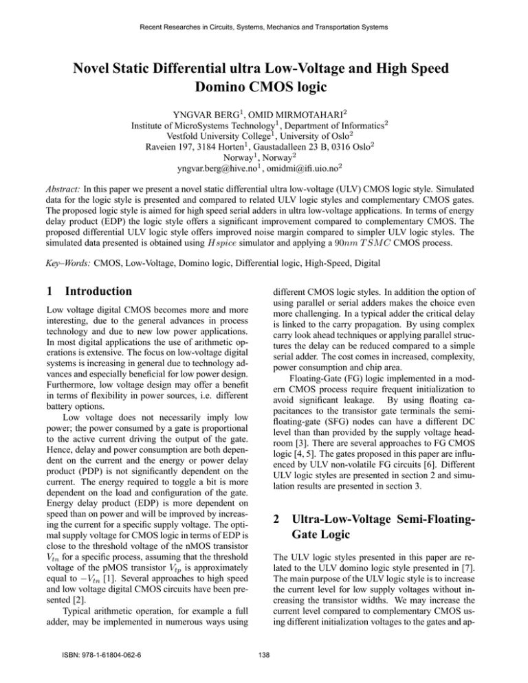
Recent Researches in Circuits, Systems, Mechanics and Transportation Systems Novel Static Differential ultra Low-Voltage and High Speed Domino CMOS logic YNGVAR BERG1 , OMID MIRMOTAHARI2 Institute of MicroSystems Technology1 , Department of Informatics2 Vestfold University College1 , University of Oslo2 Raveien 197, 3184 Horten1 , Gaustadalleen 23 B, 0316 Oslo2 Norway1 , Norway2 yngvar.berg@hive.no1 , omidmi@ifi.uio.no2 Abstract: In this paper we present a novel static differential ultra low-voltage (ULV) CMOS logic style. Simulated data for the logic style is presented and compared to related ULV logic styles and complementary CMOS gates. The proposed logic style is aimed for high speed serial adders in ultra low-voltage applications. In terms of energy delay product (EDP) the logic style offers a significant improvement compared to complementary CMOS. The proposed differential ULV logic style offers improved noise margin compared to simpler ULV logic styles. The simulated data presented is obtained using Hspice simulator and applying a 90nm T SM C CMOS process. Key–Words: CMOS, Low-Voltage, Domino logic, Differential logic, High-Speed, Digital 1 Introduction different CMOS logic styles. In addition the option of using parallel or serial adders makes the choice even more challenging. In a typical adder the critical delay is linked to the carry propagation. By using complex carry look ahead techniques or applying parallel structures the delay can be reduced compared to a simple serial adder. The cost comes in increased, complexity, power consumption and chip area. Floating-Gate (FG) logic implemented in a modern CMOS process require frequent initialization to avoid significant leakage. By using floating capacitances to the transistor gate terminals the semifloating-gate (SFG) nodes can have a different DC level than than provided by the supply voltage headroom [3]. There are several approaches to FG CMOS logic [4, 5]. The gates proposed in this paper are influenced by ULV non-volatile FG circuits [6]. Different ULV logic styles are presented in section 2 and simulation results are presented in section 3. Low voltage digital CMOS becomes more and more interesting, due to the general advances in process technology and due to new low power applications. In most digital applications the use of arithmetic operations is extensive. The focus on low-voltage digital systems is increasing in general due to technology advances and especially beneficial for low power design. Furthermore, low voltage design may offer a benefit in terms of flexibility in power sources, i.e. different battery options. Low voltage does not necessarily imply low power; the power consumed by a gate is proportional to the active current driving the output of the gate. Hence, delay and power consumption are both dependent on the current and the energy or power delay product (PDP) is not significantly dependent on the current. The energy required to toggle a bit is more dependent on the load and configuration of the gate. Energy delay product (EDP) is more dependent on speed than on power and will be improved by increasing the current for a specific supply voltage. The optimal supply voltage for CMOS logic in terms of EDP is close to the threshold voltage of the nMOS transistor Vtn for a specific process, assuming that the threshold voltage of the pMOS transistor Vtp is approximately equal to −Vtn [1]. Several approaches to high speed and low voltage digital CMOS circuits have been presented [2]. Typical arithmetic operation, for example a full adder, may be implemented in numerous ways using ISBN: 978-1-61804-062-6 2 Ultra-Low-Voltage Semi-FloatingGate Logic The ULV logic styles presented in this paper are related to the ULV domino logic style presented in [7]. The main purpose of the ULV logic style is to increase the current level for low supply voltages without increasing the transistor widths. We may increase the current level compared to complementary CMOS using different initialization voltages to the gates and ap- 138 Recent Researches in Circuits, Systems, Mechanics and Transportation Systems voltage is made stronger than the other E transistor. plying capacitive inputs. The extra loads represented by the floating capacitors are less than extra the load given by increased transistor widths. The capacitive inputs lower the delay through increased transconductance while increased transistor widths only reduce parasitic delay. The ULV logic styles may be used in critical sub circuits where high speed and low supply voltage is required. The ULV logic styles may be used together with more conventional CMOS logic. A ULV high speed serial carry chain [8] has been presented using a simple dynamic ULV logic [9]. In this paper we exploit an NP domino ULV static differential logic style. In Fig. 1 b) keeper transistors Kp and Kn are included to reduce static power and increase noise margin. The keeper transistor will reset the non-active transistor and hence reducing the static current which matches the OFF current in a complementary CMOS inverter. A simple model for the noise margin is given by N M = Ion /Iof f . Thus, by adding keepers we may increase the noise margin for the static ULV logic compared to complementary CMOS. A severe problem when using the static ULV logic, shown in Fig. 1, in carry chains is that the output is floating until an input transition occurs. If the output for some reason, noise or mismatch, starts an erroneous transition the gate will eventually be locked in a false state and will not respond to a slow input transition. We may overcome this problem by applying a differential scheme where two gates enable each other at the right time. VoffsetVoffset- Rn φ Cinp Ep Rn φ Cinp Ep Kp Vout Vin Rp Voffset+ Vout φ φ En Cinn φ Vin 2.1 Static Differential Ultra Low-Voltage Logic Kn En Cinn φ Rp φ φ Ep Voffset+ a) Dynamic ULV Ep b) Static ULV B A Figure 1: a) simple ULV inverter and b) static ULV domino logic inverter. A B The simple dynamic ULV inverter is shown in Fig. 1 a) and the static ULV inverter is shown in Fig. 1 b). There are two ways to configure these inverters: En En φ φ 1. Apply clock signals to power the inverter, i.e. connect transistor En to φ and Ep to φ and precharge the output to VDD /2 (=1/2) when φ = 1. This is called precharge or recharge mode due to the recharge of the gates through the recharge transistor Rn and Rp . The gate will be forced to 0 or 1 in the evaluation mode depending on the input transition. Voffset+ Voffset+ Figure 2: Static differential ULV NP domino (SDNPU) inverter. The static differential NP domino ULV logic is shown in Fig. 2. If we apply φ to the En transistors and VDD to the Ep transistors we precharge both outputs to logic 1 in the recharge mode, hence B = B. The pMOS keepers will be turned off and the nMOS keepers will be turned on holding the initial recharge value of the nMOS transistor. The only way to turn the keepers ON is to pull one of the outputs towards 0. Furthermore, the SDNPU inverter is suitable for large 2. Apply a clock signal to power the inverter, i.e. either φ to En and VDD to Ep , or φ to Ep and GN D to En and precharge to 1 or 0 respectively. The gate resembles NP domino logic. In order to hold the precharged value until an input transition arrives the E transistor connected to a supply ISBN: 978-1-61804-062-6 Voffset- Voffset- 139 Recent Researches in Circuits, Systems, Mechanics and Transportation Systems logic depths. The good noise margin secures stable signal values with insignificant static power consumption. The different ULV logic styles are defined by the applied terminal inputs as shown in Table 1. The ON and OFF currents of a complementary CMOS inverter is given by the effective gate source voltages VDD and 0V respectively. Assuming Cin CT = 0.5 where CT is the total capacitance seen by a floating gate, we may estimate the delay, dynamic and static power and noise margins of the different ULV logic styles relative to a complementary CMOS inverter. each logic style. The ULV inverters are first latched and then passed through a chain of 10 inverters. The simulated data is compared to the delay of a chain of complementary CMOS inverters where the total delay through a specific number of inverters corresponds to the operating frequency of the ULV inverter chain. Average values per gate are presented in this section. 2.2 Domino and Latch Configurations φ φ Vout Vin Vout φ Domino Vin φ Vin φ Vout Vin Vout 2.2 Recharge power 2 1.8 1.6 1.4 1.2 Static power 1 Switching energy 0.8 0.6 Wait energy 0.4 φ φ φ φ φ φ φ Power and energy relative to a complementary inverter 2.4 0.2 0.22 0.24 0.26 0.28 0.3 0.32 VDD [V] 0.34 0.36 0.38 0.4 LATCH LATCH φ φ φ Vout Vin Vout Vin φ φ φ Figure 4: Average relative energy and static power con- φ sumption per gate for different supply voltages. Domino Vin φ φ Vout Vin Vout φ φ φ Figure 3: Different configurations of static differential ULV logic inverters. The different configurations of static differential ULV logic inverters are shown in Fig. 3. By inverting the clock signals we obtain a latch configuration. The latched signal is available through a gate leaving the evaluation mode and entering the recharge mode. The edge created in the precharge process forces the next gate to respond to the edge and the output will be equal to the latched state. However, the delay of the first gate responding to a latched value will be large compared to the delay further down the chain. The reason for this increased delay is the time required to precharge. 3 Simulation Results The data presented is based on a 90nm TSMC CMOS process and the load applied is an identical gate for ISBN: 978-1-61804-062-6 140 The average energy per gate of the static differential NP domino ULV (SDNPU) inverter relative to a complementary inverter is shown in Fig. 4. The dynamic or switching energy of the SDNPU is close to the switching energy of a complementary CMOS inverter operating at the same supply voltage. During the time in evaluation mode before a gate toggles the gate waits in a biased state. The energy required to hold the precharged state relative to the switching energy of a complementary inverter switching is shown in Fig. 4 and labeled W ait. The relative static power and recharge power compared to static energy of a complementary is also shown for different supply voltages. As expected the power required to hold the recharged/precharged value exceeds the power required for a complementary inverter to hold a stable state. The average relative delay per gate of the ULV logic inverter chain is shown in Fig. 5. In general the simple dynamic versions are faster than their static versions due to less loads. The DNPU and SDNPU logic style is very fast due to the large current level given by the effective gate-source voltage equal to 3VDD /2. Compared to complementary CMOS the delay of the differential ULV inverters are less than 10% of a complementary CMOS inverter. The average relative energy of the ULV logic in- Recent Researches in Circuits, Systems, Mechanics and Transportation Systems ∆V Ep ± VDD 2 ± VDD 2 En φ φ VDD VDD −VDD −VDD Kp φ φ φ φ VDD VDD – B GND GND φ φ – B – B Kn Vgs ION Vgs IOF F NM∗ Style Comment – B 5VDD 4 5VDD 4 3VDD 2 3VDD 2 3 VDD 2 3VDD 2 3VDD 4 VDD 2 5VDD 4 DU SDU Dynamic Static differential VDD 3VDD 2 DNU SDNU DPU SDPU Dynamic prech. 0 Static differential prech. 0 Dynamic prech. 1 Static differential prech. 1 – B – B 0 VDD 2 0 VDD 2 VDD 3VDD 2 0 Table 1: ULV logic styles. ∆V is the output voltage swing. The simple model for the noise margin N M ∗ is given by the ratio of the ON current and the OFF current. The capacitive division factor, floating gate is assumed to be 0.5. Average delay per gate relative to an inverter 10 Cin CT where CT is the total capacitance seen by a 0 Relative average PDP per gate 1.3 1.2 SDU 1.1 SDU 1 10 0.9 −1 DU DU 0.8 SDNPU 0.7 DNPU 0.6 SDNPU 0.5 10 0.4 −2 0.2 0.22 0.24 0.26 0.28 0.3 VDD [V] 0.32 0.34 0.36 0.38 DNPU 0.4 0.2 0.22 0.24 0.26 0.28 0.3 0.32 VDD [V] 0.34 0.36 0.38 0.4 Figure 5: Average relative delay per gate of the ULV logic inverter chain. Figure 6: Average relative energy of the ULV logic inverters. verters for different supply voltages is shown in Fig. 6. The power-delay-product (PDP) of the differential gates will be increased compared to the nondifferential gates due to more complex circuitry and to the local feedback to the floating-gates. The SDU logic style has an average PDP larger than complementary CMOS. The average relative energy delay product (EDP) of the ULV logic inverters is shown in Fig. 7. The dynamic ULV gates are characterized by low EDP compared to static ULV versions. Furthermore, the differential logic styles are preferable due to low EDP. The EDP of the static differential ULV inverter is only 4% of the EDP of a complementary inverter. The noise margin for the ULV logic styles relative to a complementary inverter is shown in Fig. 8. As expected the noise margins for the static ULV inverters are improved compared to complementary CMOS for low supply voltages while the noise margins for ISBN: 978-1-61804-062-6 the dynamic gates are worse than for complementary CMOS. The relative noise margin for the dynamic ULV gates will be reduced when the supply voltage is increased due to the large OFF current of the dynamic ULV gates. The power consumed by the clock drivers are not included and must be taken into consideration for each specific application. Whenever latching is required the clock signals must be provided. The ULV logic styles can be compared to precharge logic in terms of clock load. The latching is however less clock demanding than conventional CMOS latches and flipflops. 141 Recent Researches in Circuits, Systems, Mechanics and Transportation Systems 10 10 2 Relative average EDP per gate 0 SDNPU 10 1 SDU 10 DU 10 0 SDU −1 SDNPU DNPU 10 −1 10 DU −2 DNPU 10 −2 10 −3 0.2 0.22 0.24 0.26 0.28 0.3 0.32 VDD [V] 0.34 0.36 0.38 0.4 10 −3 0.2 0.22 0.24 0.26 0.28 0.3 VDD [V] 0.32 0.34 0.36 0.38 0.4 Figure 7: Average relative energy delay product (EDP) of Figure 8: The noise margin for the ULV logic styles rela- the ULV logic inverters. tive to a complementary inverter. 4 Conclusion [5] T. Shibata and T. Ohmi. “ A Functional MOS Transistor Featuring Gate-Level Weighted Sum and Threshold Operations”, In IEEE Transactions on Electron Devices, vol 39, 1992. We have presented different ultra low-voltage (ULV) CMOS binary logic styles. The static differential ULV logic style can be used for low-voltage high-speed digital systems, and may be used together with standard low-voltage CMOS. The energy delay product of the static differential inverter is less than 10% of complementary inverters as shown in Fig. 7. [6] Y. Berg, Tor S. Lande and Ø. Næss. “Programming Floating-Gate Circuits with UV-Activated Conductances”, IEEE Transactions on Circuits and Systems -II: Analog and Digital Signal Processing, vol 48, no. 1,pp 12-19, 2001. [7] Y. Berg “Novel Ultra Low-Voltage and High Speed Domino CMOS Logic”, In proc. IEEE/IFIP International Conference on VLSI and system-on-Chip (VLSI-SoC), Madrid 27-29 september 2010. References: [1] Chandrakasan A.P. Sheng S. Brodersen R.W.: “Low-power CMOS digital design” , IEEE Journal of Solid-State Circuits, Volume 27, Issue 4, April 1992 Page(s):473 - 484 [8] Y. Berg “Ultra Low Voltage Static Carry Generate Circuit”, In Proc. IEEE International Symposium on Circuits and Systems (ISCAS), Paris, may 2010. [2] Verma N. Kwong J. Chandrakasan A.P.: “Nanometer MOSFET Variation in Minimum Energy Subthreshold Circuits” , IEEE Transactions on Electron Devices, Vol. 55, NO. 1, January 2008 Page(s):163 - 174 [9] Y. Berg: “Static Ultra Low Voltage CMOS Logic”, In Proc. IEEE NORCHIP Conference, Trondheim, NORWAY, november 2009. [3] Y. Berg, D. T. Wisland and T. S. Lande: “Ultra Low-Voltage/Low-Power Digital Floating-Gate Circuits”, IEEE Transactions on Circuits and Systems, vol. 46, No. 7, pp. 930–936,july 1999. [4] K. Kotani, T. Shibata, M. Imai and T. Ohmi. “Clocked-Neuron-MOS Logic Circuits Employing Auto-Threshold-Adjustment”, In IEEE International Solid-State Circuits Conference (ISSCC), pp. 320-321,388, 1995. ISBN: 978-1-61804-062-6 142


