RT8458
advertisement

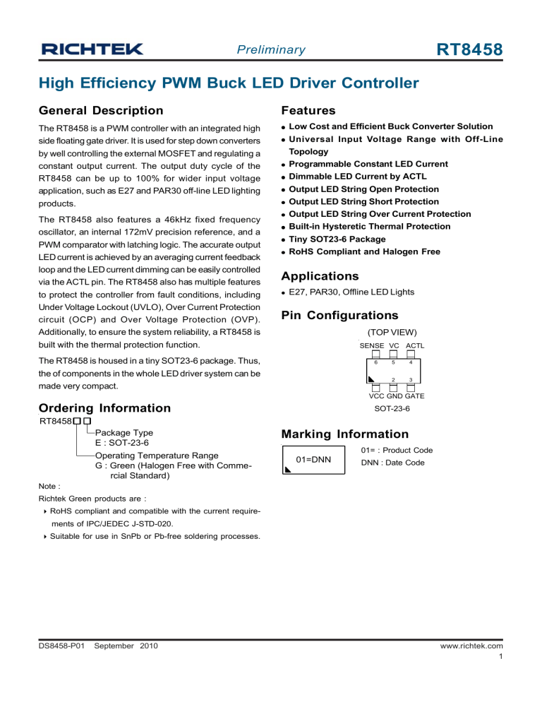
RT8458 Preliminary High Efficiency PWM Buck LED Driver Controller General Description Features The RT8458 is a PWM controller with an integrated high side floating gate driver. It is used for step down converters by well controlling the external MOSFET and regulating a constant output current. The output duty cycle of the RT8458 can be up to 100% for wider input voltage application, such as E27 and PAR30 off-line LED lighting products. z Low Cost and Efficient Buck Converter Solution z Universal Input Voltage Range with Off-Line Topology Programmable Constant LED Current Dimmable LED Current by ACTL Output LED String Open Protection Output LED String Short Protection Output LED String Over Current Protection Built-in Hysteretic Thermal Protection Tiny SOT23-6 Package RoHS Compliant and Halogen Free The RT8458 also features a 46kHz fixed frequency oscillator, an internal 172mV precision reference, and a PWM comparator with latching logic. The accurate output LED current is achieved by an averaging current feedback loop and the LED current dimming can be easily controlled via the ACTL pin. The RT8458 also has multiple features to protect the controller from fault conditions, including Under Voltage Lockout (UVLO), Over Current Protection circuit (OCP) and Over Voltage Protection (OVP). Additionally, to ensure the system reliability, a RT8458 is built with the thermal protection function. z z z z z z z z Applications z E27, PAR30, Offline LED Lights Pin Configurations (TOP VIEW) SENSE VC ACTL The RT8458 is housed in a tiny SOT23-6 package. Thus, the of components in the whole LED driver system can be made very compact. 6 5 4 2 3 VCC GND GATE Ordering Information SOT-23-6 RT8458 Package Type E : SOT-23-6 Operating Temperature Range G : Green (Halogen Free with Commercial Standard) Marking Information 01= : Product Code 01=DNN DNN : Date Code Note : Richtek Green products are : ` RoHS compliant and compatible with the current requirements of IPC/JEDEC J-STD-020. ` Suitable for use in SnPb or Pb-free soldering processes. DS8458-P01 September 2010 www.richtek.com 1 RT8458 Preliminary Typical Application Circuit 10µF 1M 1M 10 4.7µF RT8458 1 VCC ACTL 3 5 VC 3.3k 2 GND 1M SENSE 6 GATE 4 Optional Optional 3.3nF LED+ LED- Figure 1. For Typical Application 330nF 1.5M 1M 1.5M 1M RT8458 1 VCC ACTL 3 C7 4.7µF/50V 5 VC C6 3.3nF R4 10k C5 1nF 2 GND SENSE 6 GATE 4 Optional Optional LED+ LED- Figure 2. For High PF Application Functional Pin Description Pin No. Pin Name Pin Function 1 VCC Power Supply Pin of the Chip. For good bypass, a ceramic capacitor near the VCC pin is required. 2 GND Ground of the Chip. 3 GATE 4 ACTL 5 VC Gate Driver for External MOSFET Switch. Analog Dimming Control. The typical effective dimming range is between 0.2V to 1.2V. PWM loop Compensation Node. 6 SENSE LED Current Sense Input Pin. Typical sensing threshold is 190mV. www.richtek.com 2 DS8458-P01 September 2010 RT8458 Preliminary Function Block Diagram + + - Chip Enable 12V 16V/7V OSC OVP + VCC 35V S GATE R 200k R + - Control Circuit VC Dimming DS8458-P01 September 2010 ACTL - SENSE + GND www.richtek.com 3 RT8458 Preliminary Absolute Maximum Ratings z z z z z z z z z z z (Note 1) Supply Input Voltage, VCC ------------------------------------------------------------------------------------------------- 40V GATE Voltage ---------------------------------------------------------------------------------------------------------------- 14V ACTL Voltage ----------------------------------------------------------------------------------------------------------------- 8V VC Voltage -------------------------------------------------------------------------------------------------------------------- 6V SENSE Voltage -------------------------------------------------------------------------------------------------------------- −0.3V to 6V Power Dissipation, PD @ TA = 25°C SOT-23-6 ---------------------------------------------------------------------------------------------------------------------- 0.4W Package Thermal Resistance (Note 2) SOT-23-6, θJA ----------------------------------------------------------------------------------------------------------------- 250°C/W Junction Temperature ------------------------------------------------------------------------------------------------------- 150°C Lead Temperature (Soldering, 10 sec.) --------------------------------------------------------------------------------- 260°C Storage Temperature Range ---------------------------------------------------------------------------------------------- −65°C to 150°C ESD Susceptibility (Note 3) HBM (Human Body Mode) ------------------------------------------------------------------------------------------------ 2kV MM (Machine Mode) -------------------------------------------------------------------------------------------------------- 200V Recommended Operating Conditions z z (Note 4) Supply Input Voltage, VCC ------------------------------------------------------------------------------------------------- 7V to 35V Junction Temperature Range ---------------------------------------------------------------------------------------------- −40°C to 125°C Electrical Characteristics (VCC = 24VDC, CLOAD = 1nF, RLOAD = 2.2Ω in series,TA = 25°C, unless otherwise specified) Parameter Symbol Test Conditions Min Typ Max Unit -- 16 -- V Input Start-Up Voltage VST Input Supply Current ICC After Start-Up, VCC = 24V -- 1.65 5 mA Input Quiescent Current IQC Before Start-Up, VCC = 15V -- 0.1 -- μA Over Voltage Protection VOVP VCC Pin -- 35 -- V Current Sense Voltage VSENSE -- 172 -- mV Switching Frequency fSW -- 46 -- kHz Oscillator Maximum Duty Cycle DMAX -- -- 100 % Minimum Turn-On Time tON(MIN) 300 -- -- ns Gate Pin Maximum Voltage VGate -- 12.5 -- V Gate Voltage High VGate_H IGate = −20mA -- 12.5 -- IGate = −100μA --- 12.5 0.75 -- 0.5 -- 10nF Load at GATE --- 150 -- ns 10nF Load at GATE -- 0.8 -- A Gate Voltage Low GATE Drive Rise and Fall Time GATE Drive Source and Sink Peak Current VGate_F IGate = 20mA IGate = 100μA -- V V To be continued www.richtek.com 4 DS8458-P01 September 2010 RT8458 Preliminary Parameter Symbol Test Conditions Min Typ Max Unit VACTL = 0 to 1.3V -- 1 VACTL = 0.2V -- 10 --- μA -- -- 0.1 V -- 1.25 -- V --- °C LED Dimming Analog Dimming ACTL Pin Input Current IACTL LED Current Off Threshold at VACTL_Off ACTL VC Threshold for PWM Switch Off VVC Thermal Protection Thermal Shutdown Temperature TSD -- 150 Thermal Shutdown Recovery TREC -- 140 °C Note 1. Stresses listed as the above "Absolute Maximum Ratings" may cause permanent damage to the device. These are for stress ratings. Functional operation of the device at these or any other conditions beyond those indicated in the operational sections of the specifications is not implied. Exposure to absolute maximum rating conditions for extended periods may remain possibility to affect device reliability. Note 2. θJA is measured in natural convection at TA = 25°C on a low effective thermal conductivity test board of JEDEC 51-3 thermal measurement standard. Note 3. Devices are ESD sensitive. Handling precaution is recommended. Note 4. The device is not guaranteed to function outside its operating conditions. DS8458-P01 September 2010 www.richtek.com 5 RT8458 Preliminary Outline Dimension H D L C B b A A1 e Symbol Dimensions In Millimeters Dimensions In Inches Min Max Min Max A 0.889 1.295 0.031 0.051 A1 0.000 0.152 0.000 0.006 B 1.397 1.803 0.055 0.071 b 0.250 0.560 0.010 0.022 C 2.591 2.997 0.102 0.118 D 2.692 3.099 0.106 0.122 e 0.838 1.041 0.033 0.041 H 0.080 0.254 0.003 0.010 L 0.300 0.610 0.012 0.024 SOT-23-6 Surface Mount Package Richtek Technology Corporation Richtek Technology Corporation Headquarter Taipei Office (Marketing) 5F, No. 20, Taiyuen Street, Chupei City 8F, No. 137, Lane 235, Paochiao Road, Hsintien City Hsinchu, Taiwan, R.O.C. Taipei County, Taiwan, R.O.C. Tel: (8863)5526789 Fax: (8863)5526611 Tel: (8862)89191466 Fax: (8862)89191465 Email: marketing@richtek.com Information that is provided by Richtek Technology Corporation is believed to be accurate and reliable. Richtek reserves the right to make any change in circuit design, specification or other related things if necessary without notice at any time. No third party intellectual property infringement of the applications should be guaranteed by users when integrating Richtek products into any application. No legal responsibility for any said applications is assumed by Richtek. www.richtek.com 6 DS8458-P01 September 2010 RT8458 Preliminary Datasheet Revision History Version P00 Date Page No. Item 2010/7/29 Description First Edition General Description Features Typical Application Circuit P01 2010/9/1 Functional Pin D escription Function Block Diagram Modify Absolute Maximum Ratings Recommended Operating Conditions Electrical Characteristics DS8458-P01 September 2010 www.richtek.com 7


