HI-5042, HI-5043, HI-5047, HI-5049, HI-5051
Data Sheet
June 16, 2016
FN3127.7
CMOS Analog Switches
Features
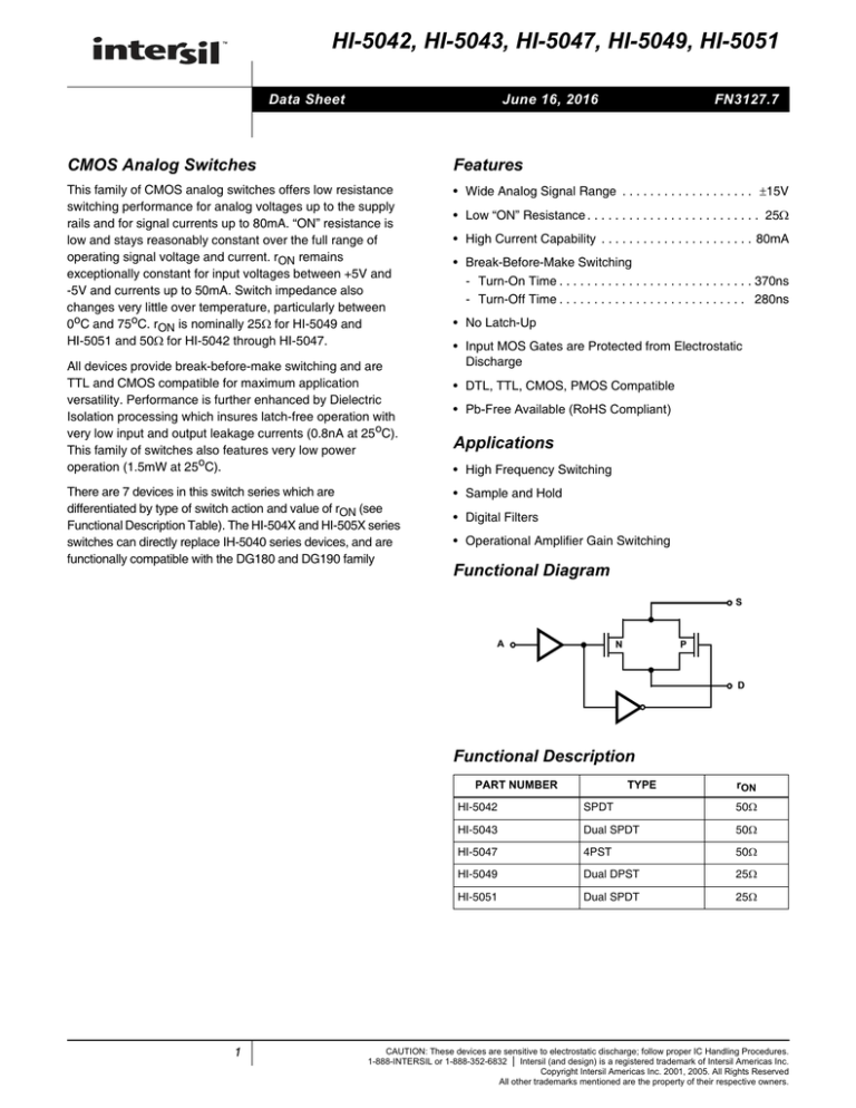
This family of CMOS analog switches offers low resistance
switching performance for analog voltages up to the supply
rails and for signal currents up to 80mA. “ON” resistance is
low and stays reasonably constant over the full range of
operating signal voltage and current. rON remains
exceptionally constant for input voltages between +5V and
-5V and currents up to 50mA. Switch impedance also
changes very little over temperature, particularly between
0oC and 75oC. rON is nominally 25 for HI-5049 and
HI-5051 and 50 for HI-5042 through HI-5047.
• Wide Analog Signal Range . . . . . . . . . . . . . . . . . . . 15V
All devices provide break-before-make switching and are
TTL and CMOS compatible for maximum application
versatility. Performance is further enhanced by Dielectric
Isolation processing which insures latch-free operation with
very low input and output leakage currents (0.8nA at 25oC).
This family of switches also features very low power
operation (1.5mW at 25oC).
There are 7 devices in this switch series which are
differentiated by type of switch action and value of rON (see
Functional Description Table). The HI-504X and HI-505X series
switches can directly replace IH-5040 series devices, and are
functionally compatible with the DG180 and DG190 family
• Low “ON” Resistance . . . . . . . . . . . . . . . . . . . . . . . . . 25
• High Current Capability . . . . . . . . . . . . . . . . . . . . . . 80mA
• Break-Before-Make Switching
- Turn-On Time . . . . . . . . . . . . . . . . . . . . . . . . . . . . 370ns
- Turn-Off Time . . . . . . . . . . . . . . . . . . . . . . . . . . . 280ns
• No Latch-Up
• Input MOS Gates are Protected from Electrostatic
Discharge
• DTL, TTL, CMOS, PMOS Compatible
• Pb-Free Available (RoHS Compliant)
Applications
• High Frequency Switching
• Sample and Hold
• Digital Filters
• Operational Amplifier Gain Switching
Functional Diagram
S
A
P
N
D
Functional Description
PART NUMBER
1
TYPE
rON
HI-5042
SPDT
50
HI-5043
Dual SPDT
50
HI-5047
4PST
50
HI-5049
Dual DPST
25
HI-5051
Dual SPDT
25
CAUTION: These devices are sensitive to electrostatic discharge; follow proper IC Handling Procedures.
1-888-INTERSIL or 1-888-352-6832 | Intersil (and design) is a registered trademark of Intersil Americas Inc.
Copyright Intersil Americas Inc. 2001, 2005. All Rights Reserved
All other trademarks mentioned are the property of their respective owners.
HI-5042 thru HI-5051
Ordering Information
TEMP. RANGE (oC)
PART NUMBER
PACKAGE
PKG. DWG. #
HI1-5042-2
-55 to 125
16 Ld CERDIP
F16.3
HI1-5043-2
-55 to 125
16 Ld CERDIP
F16.3
HI1-5043-5
0 to 75
16 Ld CERDIP
F16.3
HI3-5043-5
0 to 75
16 Ld PDIP
E16.3
HI3-5043-5Z
(See Note)
0 to 75
16 Ld PDIP*
(Pb-free)
F16.3
HI9P5043-5
0 to 75
16 Ld SOIC
M16.15
HI9P5043-5Z
(See Note)
0 to 75
16 Ld SOIC
(Pb-free)
M16.15
HI1-5047-5
0 to 75
16 Ld CERDIP
F16.3
HI1-5049-5
0 to 75
16 Ld CERDIP
F16.3
HI1-5051-2
-55 to 125
16 Ld CERDIP
F16.3
HI1-5051-5
0 to 75
16 Ld CERDIP
F16.3
HI3-5051-5
0 to 75
16 Ld PDIP
E16.3
HI3-5051-5Z (No longer available, recommended
replacement: HI9P5051-9Z (See Note)
0 to 75
16 Ld PDIP *
(Pb-free)
E16.3
HI9P5051-9
-40 to 85
16 Ld SOIC
M16.15
HI9P5051-9Z
(See Note)
-40 to 85
16 Ld SOIC
(Pb-free)
M16.15
*Pb-free PDIPs can be used for through hole wave solder processing only. They are not intended for use in Reflow solder processing applications.
NOTE: Intersil Pb-free products employ special Pb-free material sets; molding compounds/die attach materials and 100% matte tin plate termination
finish, which are RoHS compliant and compatible with both SnPb and Pb-free soldering operations. Intersil Pb-free products are MSL classified at
Pb-free peak reflow temperatures that meet or exceed the Pb-free requirements of IPC/JEDEC J STD-020.
Pinouts
(SWITCHES SHOWN FOR LOGIC “0” INPUT)
Single Control
(SWITCHES SHOWN FOR LOGIC “0” INPUT)
Dual Control
SPDT
HI-5042 (50)
4PST
HI-5047 (50)
16 S1
15 A
D2 1
2
D2 3
14 V-
S2 4
5
13 VR
12 VL
6
11 V+
7
10
7
8
9
D3 8
D1 1
Pinouts
DUAL SPDT
HI-5043 (50), HI-5051 (25)
D1 1
16 S1
D1 1
16 S1
2
16 S2
15 A
2
15 A1
2
15 A1
D1 3
14 V-
D3 3
14 V-
D3 3
14 V-
S1 4
13 VR
S3 4
13 VR
S3 4
13 VR
S4 5
D4 6
12 VL
11 V+
S4 5
D4 6
12 VL
11 V+
S4 5
12 VL
D4 6
11 V+
7
10 A2
7
10 A2
D2 8
9 S2
D2 8
9 S2
10
9 S3
NOTE: Unused pins may be internally connected. Ground all
unused pins.
2
DUAL DPST
HI-5049 (25)
NOTE: Unused pins may be internally connected. Ground all
unused pins.
HI-5042 thru HI-5051
Switch Functions
(SWITCHES SHOWN FOR LOGIC “1” INPUT)
SPDT
HI-5042 (50)
VL
12
S1
S2
A
DUAL SPDT
HI-5043 (50)
V+
VL
12
11
16
1
4
D1
S1
S3
3
D2
A1
A2
S2
15
S4
13
VR
12
S1
S2
S3
S4
A
10
9
5
13
14
VR
3
D1
D3
8
6
D2
D4
14
V-
DUAL DPST
HI-5049 (25)
V+
VL
12
11
3
16
1
9
8
5
6
15
D1
S1
D2
S3
D3
D4
A1
A2
S2
S4
VR
1
15
V-
4
13
11
16
4
4PST
HI-5047 (50)
VL
V+
14
VL
12
11
1
4
15
3
D1
D3
S1
S3
A1
10
9
5
8
6
VR
3
V+
16
13
V-
DUAL SPDT
HI-5051 (25)
14
V-
D2
D4
A2
S2
S4
V+
11
16
1
4
15
3
D1
D3
8
6
D2
10
9
5
13
VR
14
V-
D4
HI-5042 thru HI-5051
Schematic Diagrams
P15
VL
V+
P16
R6
QP6
25A
QP5
25A
QP4
100A
QP3
QN1
QP1
N13
25A
35A
P14
R3
R4
R2
R5
QP7
VR
QN2
TO VR’
25A
V+
25A
QP8
16A
P13
R7
QP2
N14
V-
N15
N16
to VL’
NOTE: Connect V+ to VL for minimizing power consumption when driving from CMOS circuits.
TTL/CMOS REFERENCE CIRCUIT (NOTE)
A1 (A2)
N1
V+
N3
IN
OUT
P2
N2
VP1
A1 (A2)
SWITCH CELL
V+
P3
P5
P1
V+
P4
N1
P6
D1
R4
P8
P7
P9
P10
P11
P12
A1
A1
VR'
A
200
D2
A2
A2
VL'
N6
V-
N7
N8
N9
P2
N4
N2
N5
N3
V-
NOTE: All N-Channel bodies to V-, all P-Channel bodies to V+ except as shown.
DIGITAL INPUT BUFFER AND LEVEL SHIFTER
4
N10
N11
N12
HI-5042 thru HI-5051
Absolute Maximum Ratings
Thermal Information
Supply Voltage (V+ to V-) . . . . . . . . . . . . . . . . . . . . . . . . . . . . . 36V
VR to Ground . . . . . . . . . . . . . . . . . . . . . . . . . . . . . . . . . . . . . . V+, VDigital and Analog Input Voltage . . . . . . . . . . . . (V+) +4V to (V-) -4V
Analog Current (S to D) Continuous . . . . . . . . . . . . . . . . . . . . 30mA
Analog Current (S to D) Peak . . . . . . . . . . . . . . . . . . . . . . . . . 80mA
Thermal Resistance (Typical, Note 1)
JA (oC/W)
JC (oC/W)
CERDIP Package. . . . . . . . . . . . . . . . .
75
22
SOIC Package . . . . . . . . . . . . . . . . . . .
110
N/A
PDIP Package* . . . . . . . . . . . . . . . . . .
90
N/A
Maximum Junction Temperature
Plastic Packages . . . . . . . . . . . . . . . . . . . . . . . . . . . . . . . . .150oC
Ceramic Packages . . . . . . . . . . . . . . . . . . . . . . . . . . . . . . . .175oC
Maximum Storage Temperature . . . . . . . . . . . . . . . -65oC to 150oC
Maximum Lead Temperature (Soldering 10s) . . . . . . . . . . . . 300oC
(SOIC - Lead Tips Only)
*Pb-free PDIPs can be used for through hole wave solder processing
only. They are not intended for use in Reflow solder processing
applications.
Operating Conditions
Temperature Range
HI-50XX-2. . . . . . . . . . . . . . . . . . . . . . . . . . . . . . . -55oC to 125oC
HI-50XX-5. . . . . . . . . . . . . . . . . . . . . . . . . . . . . . . . . . 0oC to 75oC
HI-50XX-9. . . . . . . . . . . . . . . . . . . . . . . . . . . . . . . . -40oC to 85oC
CAUTION: Stresses above those listed in “Absolute Maximum Ratings” may cause permanent damage to the device. This is a stress only rating and operation of the
device at these or any other conditions above those indicated in the operational sections of this specification is not implied.
NOTE:
1. JA is measured with the component mounted on an evaluation PC board in free air.
Electrical Specifications
Supplies = +15V, -15V; VR = 0V; VAH (Logic Level High) = 2.4V, VAL (Logic Level Low) = 0.8V, VL = 5V,
Unless Otherwise Specified. For Test Conditions, Consult Performance Characteristics,
Unused Pins are Grounded
TEST
CONDITIONS
PARAMETER
-2
-5, -9
TEMP
(oC)
MIN
TYP
MAX
MIN
TYP
MAX
UNITS
25
-
370
500
-
370
500
ns
DYNAMIC CHARACTERISTICS
(Note 5)
Switch ON Time, tON
Switch OFF Time, tOFF
(Note 5)
25
-
280
500
-
280
500
ns
Charge Injection, Q
(Note 3)
25
-
5
20
-
5
-
mV
OFF Isolation
(Note 4)
25
75
80
-
-
80
-
dB
Crosstalk
(Note 4)
25
-80
-88
-
-
-88
-
dB
Input Switch Capacitance, CS(OFF)
25
-
11
-
-
11
-
pF
Output Switch Capacitance, CD(OFF)
25
-
11
-
-
11
-
pF
Output Switch Capacitance, CD(ON)
25
-
22
-
-
22
-
pF
Digital Input Capacitance, CA
25
-
5
-
-
5
-
pF
Drain To Source Capacitance, CDS(OFF)
25
-
0.5
-
-
0.5
-
pF
Input Low Threshold, VAL
Full
-
-
0.8
-
-
0.8
V
Input High Threshold, VAH
Full
2.4
-
-
2.4
-
-
V
Input Leakage Current (High or Low), IA
Full
-
0.01
1.0
-
0.01
1.0
A
Full
-15
-
+15
-15
-
+15
V
25
-
50
75
-
50
75
Full
-
-
150
-
-
150
DIGITAL INPUT CHARACTERISTICS
ANALOG SWITCH CHARACTERISTICS
Analog Signal Range
ON Resistance, rON
HI-5042 to HI-5047
(Note 2)
25
-
25
45
-
25
45
Full
-
-
50
-
-
50
HI-5042 to HI-5047
25
-
2
10
-
2
10
HI-5049, HI-5051
25
-
1
5
-
1
5
HI-5049, HI-5051
(Note 2)
Channel-to-Channel Match, rON
5
HI-5042 thru HI-5051
Electrical Specifications
Supplies = +15V, -15V; VR = 0V; VAH (Logic Level High) = 2.4V, VAL (Logic Level Low) = 0.8V, VL = 5V,
Unless Otherwise Specified. For Test Conditions, Consult Performance Characteristics,
Unused Pins are Grounded (Continued)
TEST
CONDITIONS
PARAMETER
-2
TEMP
(oC)
MIN
TYP
-5, -9
MAX
MIN
TYP
MAX
UNITS
OFF Input or Output Leakage Current,
IS(OFF) = ID(OFF)
25
-
0.8
2
-
0.8
2
nA
Full
-
100
200
-
100
200
nA
ON Leakage Current, ID(ON)
25
-
0.01
2
-
0.01
2
nA
Full
-
2
200
-
2
200
nA
Quiescent Power Dissipation, PD
25
-
1.5
-
-
1.5
-
mW
I+, I-, IL , IR
25
-
-
0.2
-
-
0.3
mA
POWER REQUIREMENTS
I+, +15V Quiescent Current
(Note 5)
Full
-
-
0.3
-
-
0.5
mA
I-, -15V Quiescent Current
(Note 5)
Full
-
-
0.3
-
-
0.5
mA
IL , +5V Quiescent Current
(Note 5)
Full
-
-
0.3
-
-
0.5
mA
IR , Ground Quiescent Current
(Note 5)
Full
-
-
0.3
-
-
0.5
mA
NOTES:
2. VOUT = 10V, IOUT =
3. VIN = 0V, CL = 10nF.
1mA.
4. RL = 100, f = 100kHz, VIN = 2.0VP-P , CL = 5pF.
5. VAL = 0V, VAH = 5V.
TA = 25oC, V+ = +15V, V- = -15V, VL = +5V, VR = 0V, VAH = 3V and VAL = 0.8V
Unless Otherwise Specified
Test Circuits and Waveforms
1mA
rON =
V2
V2
1mA
IN
OUT
VIN
FIGURE 1A. TEST CIRCUIT
NORMALIZED ON RESISTANCE
(REFERRED TO 25oC)
ON RESISTANCE ()
80
60
V+ = +12V
V- = -12V
V+ = +10V
V- = -10V
40
20
0
-15
V+ = +15V
V- = -15V
1.2
1.1
1.0
0.9
0.8
0.7
0.6
-10
0
-5
5
10
15
-25
0
25
50
75
100
125
FIGURE 1C. NORMALIZED ON RESISTANCE vs TEMPERATURE
FIGURE 1. ON RESISTANCE
6
-50
TEMPERATURE (oC)
ANALOG SIGNAL LEVEL (V)
FIGURE 1B. ON RESISTANCE vs ANALOG SIGNAL LEVEL
VIN = 0V
HI-5042 thru HI-5051
Test Circuits and Waveforms
TA = 25oC, V+ = +15V, V- = -15V, VL = +5V, VR = 0V, VAH = 3V and VAL = 0.8V
Unless Otherwise Specified (Continued)
OFF LEAKAGE CURRENT
100nA
A
IS(OFF) = ID(OFF)
10nA
ID(OFF)
IN
OUT
A
10V
LEAKAGE CURRENT
IS(OFF)
10V
ON LEAKAGE CURRENT
1nA
IN
OUT
ID(ON)
100pA
A
ID(ON)
10V
10pA
25
50
75
100
125
TEMPERATURE (oC)
FIGURE 2A. LEAKAGE CURRENTS vs TEMPERATURE
FIGURE 2B. TEST CIRCUITS
FIGURE 2. LEAKAGE CURRENTS
NORMALIZED ON RESISTANCE
(REFERRED TO 1mA)
1.4
1.3
1.2
IN
VIN
1.1
OUT
I
V IN
r ON = --------I
1.0
0
20
40
60
80
ANALOG CURRENT (mA)
FIGURE 3A. NORMALIZED ON RESISTANCE vs ANALOG
CURRENT
FIGURE 3B. TEST CIRCUIT
FIGURE 3. NORMALIZED ON RESISTANCE
OFF ISOLATION (dB)
200
IN
160
VIN
2VP-P
RL = 100
120
80
1
10
100
1K
10K
50
V IN
OFF ISOLATION = 20 Log ----------------
V OUT
RL = 10k
40
OUT
100K
1M
FREQUENCY (Hz)
FIGURE 4A. OFF ISOLATION vs FREQUENCY
FIGURE 4C. OFF ISOLATION
7
FIGURE 4B. TEST CIRCUIT
RL
VOUT
HI-5042 thru HI-5051
TA = 25oC, V+ = +15V, V- = -15V, VL = +5V, VR = 0V, VAH = 3V and VAL = 0.8V
Unless Otherwise Specified (Continued)
Test Circuits and Waveforms
CROSSTALK (dB)
-200
SWITCHED
CHANNEL
-160
VIN
-120
50
2VP-P
RL = 100
VOUT
RL
-80
RL = 1k
RL = 10k
-40
0
RL
1
10
100
1K
10K
100K
V OUT
CROSSTALK = 20 Log ----------------
V IN
1M
FREQUENCY (Hz)
FIGURE 5A. CROSSTALK vs FREQUENCY
FIGURE 5B. TEST CIRCUIT
FIGURE 5. CROSSTALK
POWER CONSUMPTION (mW)
200
160
+10V
-10V
120
TOGGLE
AT 50%
DUTY
80
A
VL VR V+
IL
I+
VI-
40
+5V
0
1K
10K
100K
+15V -15V
1M
TOGGLE FREQUENCY (50% DUTY CYCLE) (Hz)
FIGURE 6A. POWER CONSUMPTION vs FREQUENCY
FIGURE 6B. TEST CIRCUIT
FIGURE 6. POWER CONSUMPTION
VAH
VA
IN1
OUT 1
90%
90%
+10V
OUT 2
IN2
1K
OUT 1
tON
tOFF
90%
1K
90%
VA
tOFF
FIGURE 7A. TEST CIRCUIT
8
tON
FIGURE 7B. MEASUREMENT POINTS
OUT 2
HI-5042 thru HI-5051
Test Circuits and Waveforms
TA = 25oC, V+ = +15V, V- = -15V, VL = +5V, VR = 0V, VAH = 3V and VAL = 0.8V
Unless Otherwise Specified (Continued)
VA
VA
OUTPUT
OUTPUT
VA = 0V to 10V
Vertical: 5V/Div.
Horizontal: 200ns/Div.
FIGURE 7D. WAVEFORMS WITH CMOS COMPATIBLE LOGIC
INPUT
720
660
660
600
600
540
540
INPUT)
720
480
420
tON
360
300
(NEED
(NEED
INPUT)
VA = 0V to 5V
Vertical: 2V/Div.
Horizontal: 200ns/Div.
FIGURE 7C. WAVEFORMS WITH TTL COMPATIBLE LOGIC
INPUT
tOFF
240
480
420
360
240
180
180
120
120
60
2.4
tON
300
tOFF
60
3.0
3.6
4.2
4.8
0
DIGITAL “HIGH” (V)
1.0
1.5
DIGITAL “LOW” (V)
FIGURE 7E. SWITCHING TIMES vs POSITIVE DIGITAL VOLTAGE
FIGURE 7F. SWITCHING TIMES vs NEGATIVE DIGITAL VOLTAGE
FIGURE 7. SWITCH tON AND tOFF
9
0.5
HI-5042 thru HI-5051
Revision History
The revision history provided is for informational purposes only and is believed to be accurate, but not warranted.
Please go to the web to make sure that you have the latest revision.
DATE
REVISION
June 16, 2016
FN3127.7
CHANGE
Updated Ordering Information table on page 2.
Added Revision History and About Intersil sections.
Updated POD M16.15 to the latest revision changes are as follows:
Remove "u" symbol from drawing (overlaps the "a" on Side View). Multiple changes were made to
table.
About Intersil
Intersil Corporation is a leading provider of innovative power management and precision analog solutions. The company's products
address some of the largest markets within the industrial and infrastructure, mobile computing and high-end consumer markets.
For the most updated datasheet, application notes, related documentation and related parts, please see the respective product
information page found at www.intersil.com.
You may report errors or suggestions for improving this datasheet by visiting www.intersil.com/ask.
Reliability reports are also available from our website at www.intersil.com/support.
10
HI-5042 thru HI-5051
Dual-In-Line Plastic Packages (PDIP)
E16.3 (JEDEC MS-001-BB ISSUE D)
N
16 LEAD DUAL-IN-LINE PLASTIC PACKAGE
E1
INDEX
AREA
1 2 3
INCHES
N/2
-B-
-AE
D
BASE
PLANE
-C-
SEATING
PLANE
A2
A
L
D1
e
B1
D1
A1
eC
B
0.010 (0.25) M
C A B S
MILLIMETERS
SYMBOL
MIN
MAX
MIN
MAX
NOTES
A
-
0.210
-
5.33
4
A1
0.015
-
0.39
-
4
A2
0.115
0.195
2.93
4.95
-
B
0.014
0.022
0.356
0.558
-
C
L
B1
0.045
0.070
1.15
1.77
8, 10
eA
C
0.008
0.014
C
D
0.735
0.775
eB
NOTES:
1. Controlling Dimensions: INCH. In case of conflict between English and
Metric dimensions, the inch dimensions control.
0.005
-
0.13
-
5
0.300
0.325
7.62
8.25
6
E1
0.240
0.280
6.10
7.11
5
e
0.100 BSC
eA
0.300 BSC
eB
-
4. Dimensions A, A1 and L are measured with the package seated in JEDEC seating plane gauge GS-3.
L
0.115
N
8. B1 maximum dimensions do not include dambar protrusions. Dambar
protrusions shall not exceed 0.010 inch (0.25mm).
9. N is the maximum number of terminal positions.
10. Corner leads (1, N, N/2 and N/2 + 1) for E8.3, E16.3, E18.3, E28.3,
E42.6 will have a B1 dimension of 0.030 - 0.045 inch (0.76 - 1.14mm).
11
5
E
2. Dimensioning and tolerancing per ANSI Y14.5M-1982.
7. eB and eC are measured at the lead tips with the leads unconstrained.
eC must be zero or greater.
0.355
19.68
D1
3. Symbols are defined in the “MO Series Symbol List” in Section 2.2 of
Publication No. 95.
5. D, D1, and E1 dimensions do not include mold flash or protrusions.
Mold flash or protrusions shall not exceed 0.010 inch (0.25mm).
6. E and eA are measured with the leads constrained to be perpendicular to datum -C- .
0.204
18.66
16
2.54 BSC
7.62 BSC
0.430
-
0.150
2.93
16
6
10.92
7
3.81
4
9
Rev. 0 12/93
HI-5042 thru HI-5051
Small Outline Plastic Packages (SOIC)
M16.15 (JEDEC MS-012-AC ISSUE C)
N
INDEX
AREA
H
0.25(0.010) M
16 LEAD NARROW BODY SMALL OUTLINE PLASTIC PACKAGE
B M
INCHES
E
-B-
1
2
3
L
SEATING PLANE
-A-
A
D
h x 45°
-C-
e
A1
B
0.25(0.010) M
C
0.10(0.004)
C A M
SYMBOL
MIN
MAX
MIN
MAX
NOTES
A
0.0532
0.0688
1.35
1.75
-
A1
0.0040
0.0098
0.10
0.25
-
B
0.013
0.020
0.33
0.51
9
C
0.0075
0.0098
0.19
0.25
-
D
0.3859
0.3937
9.80
10.00
3
E
0.1497
0.1574
3.80
4.00
4
e
B S
1. Symbols are defined in the “MO Series Symbol List” in Section 2.2 of
Publication Number 95.
2. Dimensioning and tolerancing per ANSI Y14.5M-1982.
3. Dimension “D” does not include mold flash, protrusions or gate burrs.
Mold flash, protrusion and gate burrs shall not exceed 0.15mm (0.006
inch) per side.
4. Dimension “E” does not include interlead flash or protrusions. Interlead
flash and protrusions shall not exceed 0.25mm (0.010 inch) per side.
5. The chamfer on the body is optional. If it is not present, a visual index
feature must be located within the crosshatched area.
6. “L” is the length of terminal for soldering to a substrate.
7. “N” is the number of terminal positions.
8. Terminal numbers are shown for reference only.
9. The lead width “B”, as measured 0.36mm (0.014 inch) or greater above
the seating plane, shall not exceed a maximum value of 0.61mm
(0.024 inch).
10. Controlling dimension: MILLIMETER. Converted inch dimensions are
not necessarily exact.
12
0.050 BSC
1.27 BSC
-
H
0.2284
0.2440
5.80
6.20
-
h
0.0099
0.0196
0.25
0.50
5
L
0.016
0.050
0.40
1.27
6
N
NOTES:
MILLIMETERS
16
0°
16
8°
0°
7
8°
Rev. 1 6/05
HI-5042 thru HI-5051
Ceramic Dual-In-Line Frit Seal Packages (CERDIP)
F16.3 MIL-STD-1835 GDIP1-T16 (D-2, CONFIGURATION A)
16 LEAD CERAMIC DUAL-IN-LINE FRIT SEAL PACKAGE
LEAD FINISH
c1
-D-
-A-
BASE
METAL
(c)
E
M
-Bbbb S
C A-B S
Q
-C-
SEATING
PLANE
S1
b2
ccc M
C A-B S
eA/2
-
0.200
-
5.08
-
0.026
0.36
0.66
2
b1
0.014
0.023
0.36
0.58
3
b2
0.045
0.065
1.14
1.65
-
b3
0.023
0.045
0.58
1.14
4
c
0.008
0.018
0.20
0.46
2
c1
0.008
0.015
0.20
0.38
3
D
-
0.840
-
21.34
5
E
0.220
0.310
5.59
7.87
5
c
aaa M C A - B S D S
D S
NOTES
0.014
eA
e
b
MAX
b
A A
MIN
A
A
L
MILLIMETERS
MAX
M
(b)
D
BASE
PLANE
MIN
b1
SECTION A-A
D S
INCHES
SYMBOL
NOTES:
1. Index area: A notch or a pin one identification mark shall be located adjacent to pin one and shall be located within the shaded
area shown. The manufacturer’s identification shall not be used
as a pin one identification mark.
e
0.100 BSC
2.54 BSC
-
eA
0.300 BSC
7.62 BSC
-
eA/2
0.150 BSC
3.81 BSC
-
L
0.125
0.200
3.18
5.08
-
Q
0.015
0.060
0.38
1.52
6
S1
0.005
-
0.13
-
7
105o
90o
105o
-
2. The maximum limits of lead dimensions b and c or M shall be
measured at the centroid of the finished lead surfaces, when
solder dip or tin plate lead finish is applied.
90o
aaa
-
0.015
-
0.38
-
3. Dimensions b1 and c1 apply to lead base metal only. Dimension
M applies to lead plating and finish thickness.
bbb
-
0.030
-
0.76
-
ccc
-
0.010
-
0.25
-
M
-
0.0015
-
0.038
2, 3
4. Corner leads (1, N, N/2, and N/2+1) may be configured with a
partial lead paddle. For this configuration dimension b3 replaces
dimension b2.
N
16
16
5. This dimension allows for off-center lid, meniscus, and glass
overrun.
8
Rev. 0 4/94
6. Dimension Q shall be measured from the seating plane to the
base plane.
7. Measure dimension S1 at all four corners.
8. N is the maximum number of terminal positions.
9. Dimensioning and tolerancing per ANSI Y14.5M - 1982.
10. Controlling dimension: INCH.
All Intersil U.S. products are manufactured, assembled and tested utilizing ISO9001 quality systems.
Intersil Corporation’s quality certifications can be viewed at www.intersil.com/design/quality
Intersil products are sold by description only. Intersil Corporation reserves the right to make changes in circuit design, software and/or specifications at any time without
notice. Accordingly, the reader is cautioned to verify that data sheets are current before placing orders. Information furnished by Intersil is believed to be accurate and
reliable. However, no responsibility is assumed by Intersil or its subsidiaries for its use; nor for any infringements of patents or other rights of third parties which may result
from its use. No license is granted by implication or otherwise under any patent or patent rights of Intersil or its subsidiaries.
For information regarding Intersil Corporation and its products, see www.intersil.com
13
