N-Channel JFET 40V, 50 to 130μA, 0.11mS, SOT-883
advertisement
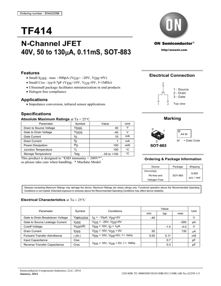
Ordering number : ENA2259B TF414 N-Channel JFET 40V, 50 to 130A, 0.11mS, SOT-883 Features http://onsemi.com Electrical Connection Small IGSS : max 500pA (VGS= 20V, VDS=0V) Small Ciss : typ 0.7pF (VDS=10V, VGS=0V, f=1MHz) Ultrasmall package facilitates miniaturization in end products Halogen free compliance 3 1 : Source 2 : Drain 3 : Gate Applications Impedance conversion, infrared sensor applications 2 1 Top view Specifications Marking Absolute Maximum Ratings at Ta = 25C Parameter Drain to Source Voltage Symbol VDSS Value Unit V Gate to Drain Voltage VGDS Gate Current IG Drain Current ID 1 mA Power Dissipation PD 100 mW Junction Temperature Tj 150 Storage Temperature Tstg C C 40 40 3 V mA 10 55 to +150 This product is designed to “ESD immunity < 200V*”, so please take care when handling. * Machine Model 1 A4 M M 2 = Date Code SOT-883 Ordering & Package Information Device Package TF414T5G Pb-free and SOT-883 Halogen Free Shipping 8,000 pcs. / reel Stresses exceeding Maximum Ratings may damage the device. Maximum Ratings are stress ratings only. Functional operation above the Recommended Operating Conditions is not implied. Extended exposure to stresses above the Recommended Operating Conditions may affect device reliability. Electrical Characteristics at Ta 25C Parameter Symbol Gate to Drain Breakdown Voltage V(BR)GDS IG = 10μA, VDS=0V Gate to Source Leakage Current IGSS VGS = 20V, VDS=0V Cutoff Voltage VGS(off) Drain Current IDSS VDS = 10V, ID = 1μA VDS = 10V, VGS = 0V Forward Transfer Admittance | yfs | VDS = 10V, VGS=0V, f = 1kHz Input Capacitance Ciss Reverse Transfer Capacitance Crss Semiconductor Components Industries, LLC, 2014 January, 2014 Conditions Value min typ max 40 VDS = 10V, VGS = 0V, f = 1MHz V 1.4 50 0.05 Unit 500 pA 4.0 V 130 0.11 A mS 0.7 pF 0.3 pF 12814HK TC-00003085/D1813HK/D1113HK GB No.A2259-1/3 TF414 ID -- VDS 120 100 VGS=0V Drain Current, ID -- μA Drain Current, ID -- μA ID -- VDS 120 80 --0.2V 60 --0.4V 40 --0.6V --0.8V 20 100 VGS=0V 80 --0.2V 60 --0.4V --0.6V 40 --0.8V 20 --1.0V --1.0V 0 0 1 2 3 4 Drain-to-Source Voltage, VDS -- V 120 ID -- VGS Cutoff Voltage, VGS(off) -- V --2 5° C 60 25 °C Ta = 40 75 °C 15 20 25 30 IT16762 VGS(off) -- IDSS VDS=10V ID=1.0μA --2.0 --1.8 --1.6 --1.4 --1.0 --0.8 0 --2.0 --1.5 --1.0 --0.5 --0.4 40 0 Gate-to-Source Voltage, VGS -- V 80 120 140 HD131113 Ciss -- VDS 1.0 VDS=10V VGS=0V f=1kHz 100 Drain Current, IDSS -- μA | yfs | -- IDSS 0.14 60 IT16764 VGS=0V f=1MHz Input Capacitance, Ciss -- pF 7 0.12 0.11 0.10 0.09 0.08 5 3 2 0.07 0.06 40 60 80 100 120 Drain Current, IDSS -- μA VGS=0V f=1MHz 7 5 3 2 2 3 5 7 1.0 2 3 5 7 10 2 3 2 3 Drain-to-Source Voltage, VDS -- V 5 7 100 IT16768 5 7 1.0 2 3 5 7 10 2 3 Drain-to-Source Voltage, VDS -- V HD131113 Crss -- VDS 1.0 0.1 0.1 0.1 0.1 140 5 7 100 IT16767 PD -- Ta 120 Allowable Power Dissipation, PD -- mW Drain Current, ID -- μA 10 --2.2 80 0.13 5 Drain-to-Source Voltage, VDS -- V VDS=10V 20 Forward Transfer Admittance, | yfs | -- mS 0 IT16761 100 Reverse Transfer Capacitance, Crss -- pF 0 5 100 80 60 40 20 0 0 20 40 60 80 100 120 Ambient Temperature, Ta -- °C 140 160 HD131212 No.A2259-2/3 TF414 Package Dimensions unit : mm SOT-883 (XDFN3), 1.0x0.6, 0.35P CASE 506CB ISSUE A NOTES: 1. DIMENSIONING AND TOLERANCING PER ASME Y14.5M, 1994. 2. CONTROLLING DIMENSION: MILLIMETERS. 3. EXPOSED COPPER ALLOWED AS SHOWN. A B D PIN ONE REFERENCE 3X 0.10 C 0.10 C 0.10 C 0.10 C E DIM A A1 b D D2 e E E2 L TOP VIEW NOTE 3 A A1 SIDE VIEW C SEATING PLANE E2 e/2 1 2X 0.10 M C AB 0.05 M C 3X b GENERIC MARKING DIAGRAM* XX M D2 e MILLIMETERS MIN MAX 0.340 0.440 0.000 0.030 0.075 0.200 0.950 1.075 0.620 BSC 0.350 BSC 0.550 0.675 0.425 0.550 0.170 0.300 XX = Specific Device Code M = Date Code *This information is generic. Please refer to device data sheet for actual part L BOTTOM VIEW RECOMMENDED SOLDER FOOTPRINT* 1.10 2X 2X 0.43 1 0.20 0.41 0.55 PACKAGE OUTLINE DIMENSIONS: MILLIMETERS *For additional information on our Pb−Free strategy and soldering details, please download the ON Semiconductor Soldering and Mounting Techniques Reference Manual, SOLDERRM/D. ON Semiconductor and the ON logo are registered trademarks of Semiconductor Components Industries, LLC (SCILLC). SCILLC owns the rights to a number of patents, trademarks, copyrights, trade secrets, and other intellectual property. A listing of SCILLC’s product/patent coverage may be accessed at www.onsemi.com/site/pdf/Patent-Marking.pdf. SCILLC reserves the right to make changes without further notice to any products herein. SCILLC makes no warranty, representation or guarantee regarding the suitability of its products for any particular purpose, nor does SCILLC assume any liability arising out of the application or use of any product or circuit, and specifically disclaims any and all liability, including without limitation special, consequential or incidental damages. “Typical” parameters which may be provided in SCILLC data sheets and/or specifications can and do vary in different applications and actual performance may vary over time. All operating parameters, including “Typicals” must be validated for each customer application by customer’s technical experts. SCILLC does not convey any license under its patent rights nor the rights of others. SCILLC products are not designed, intended, or authorized for use as components in systems intended for surgical implant into the body, or other applications intended to support or sustain life, or for any other application in which the failure of the SCILLC product could create a situation where personal injury or death may occur. Should Buyer purchase or use SCILLC products for any such unintended or unauthorized application, Buyer shall indemnify and hold SCILLC and its officers, employees, subsidiaries, affiliates, and distributors harmless against all claims, costs, damages, and expenses, and reasonable attorney fees arising out of, directly or indirectly, any claim of personal injury or death associated with such unintended or unauthorized use, even if such claim alleges that SCILLC was negligent regarding the design or manufacture of the part. SCILLC is an Equal Opportunity/Affirmative Action Employer. This literature is subject to all applicable copyright laws and is not for resale in any manner. PS No.A2259-3/3 Mouser Electronics Authorized Distributor Click to View Pricing, Inventory, Delivery & Lifecycle Information: ON Semiconductor: TF414T5G
