Evaluation Board User Guide
UGOne Technology Way • P.O. Box 9106 • Norwood, MA 02062-9106, U.S.A. • Tel: 781.329.4700 • Fax: 781.461.3113 • www.analog.com
Evaluation Board for Fractional-N/Integer-N PLL Frequency Synthesizer
synthesizer, a USB connector and related interface, SMA
connectors for the RF outputs, and reference signal plus headers
for various signals and voltages. There is also a loop filter
(5 kHz) on board. An SDP-S connector is required to operate
the board, this is ordered separately.
FEATURES
Self-contained board including PLL, VCO, loop filter (3 kHz),
USB interface, and voltage regulators
Accompanying software allows control of synthesizer
functions from a PC
Choice of power supply via USB or external feeding
Typical phase noise performance of −111 dBc/Hz @ 100 kHz
offset from carrier (6.8 GHz output frequency)
The package also contains Windows® software (XP, Vista-and
Windows 7 compatible) to allow easy programming of the
synthesizer.
GENERAL DESCRIPTION
EVALUATION KIT CONTENTS
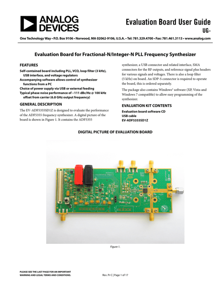
The EV-ADF5355SD1Z is designed to evaluate the performance
of the ADF5355 frequency synthesizer. A digital picture of the
board is shown in Figure 1. It contains the ADF5355
Evaluation board software CD
USB cable
EV-ADF5355SD1Z
DIGITAL PICTURE OF EVALUATION BOARD
Figure 1.
PLEASE SEE THE LAST PAGE FOR AN IMPORTANT
WARNING AND LEGAL TERMS AND CONDITIONS.
Rev. Pr C | Page 1 of 17
UG-
Evaluation Board User Guide
TABLE OF CONTENTS
Features .............................................................................................. 1 Power Supplies ...............................................................................3 General Description ......................................................................... 1 RF Output .......................................................................................3 Evaluation Kit Contents ................................................................... 1 Loop Filter ......................................................................................3 Digital Picture of Evaluation Board ............................................... 1 Reference Source ...........................................................................3 Revision History ............................................................................... 2 Evaluation Set Up ..............................................................................4 Evaluation Board Hardware ............................................................ 3 Evaluation Board Software ...............................................................5 Overview........................................................................................ 3 Evaluation Board Schematics and Artwork ...................................9 REVISION HISTORY
14/10—Revision PrC: Updated for revised components.
14/07—Revision PrB: Initial Preliminary Version
Edited description.
14/05—Revision PrA: Initial Preliminary Version
Rev. Pr C | Page 2 of 17
Evaluation Board User Guide
UG-
EVALUATION BOARD HARDWARE
Figure 2. Customers wishing for lowest noise at 100 kHz offset
are advised to use the following components, and to use 0.9 mA
charge pump current, which are inserted on the evaluation
board.
OVERVIEW
The EV-ADF5355SD1Z requires the SPD-S platform which
uses the EVAL-SDP-CS1Z. (SDP-B is not recommended).
POWER SUPPLIES
C60 = 22 nF, C59 = 0.47 uF, C14 = 10 nF, C73 = 10 pF.
The EV-ADF5355SD1Zis powered from dc power connectors
(4 mm banana connectors). When feeding via banana
connectors, 6.0 V is a suitable feeding voltage. The power
supply circuitry allows the user to use two or three separate
LDOs to feed the ADF5355 (using fewer LDOs increases the
risk of spur contaminated dc feeds). Ensure the switch is in the
correct position to power the board. Consult the board
schematic in Figure 20, Figure 21, and Figure 22 to determine a
suitable setting.
R14 = 220 Ohms, R1 = 470 Ohms.
Customers wishing for lowest rms phase noise should use:
C60 = 1.2 nF, C59 = 33 nF, C14 = 390 pF, C73 = 10 pF.
R14 = 1 kOhms, R17 = 3.3 kOhm.
And also program the 0.9 mA charge pump current.
The charge pump and VCO supply pins are driven from a 5V
ADM7150 high performance low noise regulator. The
remaining supplies are powered from 3.3V ADM7150’s.
An LED, indicates when USB power is available, and another
LED, indicates when the ADF5355 is powered on. Switch S1 is
used to power the ADF5355 from the external dc connectors,
and should be switched to the left.
In case the SDP processor causes spurs on the RF output signal,
the user may remove this connector and measure the spurious.
Figure 2. Loop Filter Placement
RF OUTPUT
REFERENCE SOURCE
The EV-ADF5355SD1Z has one pair of SMA output connectors
(differential outputs RFoutA+/-). The device is quite sensitive to
impedance unbalance. If only one port of a differential pair is
used, terminate the other with a 50 Ω load. If only RFoutB is
used, then it can be powered off, or if left on, both RFoutA pins
should be terminated in 50 Ohms.
The evaluation board contains a footprint for a 122.88 MHz
differential output TCXO from Vectron. If preferred, the user
may supply either a single-ended or differential reference input
to connectors REFINA and REFINB. Disconnect the power rail
to the TCXO by removing resistor R12 first.
The RFoutB contains the high frequency (6.8 – 13.6 GHz) and
is a single ended RF output.
LOOP FILTER
The loop filter schematic is included in the board schematic on
Figure 20. The loop filter component placements are clarified in
To use a single ended REFIN, then connect a low noise 122.88
MHz reference source to REFINB. To use a differential REFIN
connect the differential signal to REFINA and REFINB. The
differential REFIN can operate to 500 MHz input frequency.
If the TCXO is removed, then an external REFIN must be used.
Rev. Pr C | Page 3 of 17
UG-
Evaluation Board User Guide
EVALUATION SET UP
50 Ohm
50 Ohm
Termination Termination
Lock detect LED
Loop filter
PC
ADF5355
External DC
supply
External DC
GND
PLL
power
LED
Spectrum
Analyzer
Reference In/Out
Power switch
Reference (optional)
TCXO
Figure 3. Evaluation Set Up
Rev. Pr C | Page 4 of 17
Evaluation Board User Guide
UGWindows XP Software Installation Guide
SOFTWARE INSTALLATION
Use the following steps to install the software.
1.
2.
Install the Analog Devices ADF4355 software by doubleclicking ADF4355 Setup.msi.
If you are using Windows XP, follow the instructions in the
Windows XP Software Installation Guide section (see
Figure 4 to Figure 8).
If you are using Windows Vista or Windows 7, follow the
instructions in the Windows Vista and Windows 7 Software
Installation Guide section (see Figure 9 to Figure 13).
Note that the software requires Microsoft Windows
Installer and Microsoft .NET Framework 3.5 (or higher).
The installer connects to the Internet and downloads
Microsoft .NET Framework automatically. Alternatively,
before running the ADF4355 Setup.msi, both the installer
and .NET Framework can be installed from the CD
provided.
Connect your board by USB.
If you are using Windows XP, follow the steps in the
Windows XP Driver Installation Guide section (see Figure 14
to Figure 17).
On Windows Vista or Windows 7, the drivers install
automatically.
Figure 4. Windows XP ADF4355 Software Installation, Setup Wizard
1.
Click Next.
Figure 5. Windows XP ADF4355 Software Installation, Select Installation
Folder
2.
Rev. Pr C | Page 5 of 17
Choose an installation directory and click Next.
UG-
Evaluation Board User Guide
5.
Click Close.
Windows Vista and Windows 7 Software Installation Guide
Figure 6. Windows XP ADF4355 Software Installation, Confirm Installation
3.
Click Next.
Figure 9. Windows Vista/7 ADF4355 Software Installation, Setup Wizard
Click Next.
10482-006
1.
Figure 7. Windows XP ADF4355 Software Installation, Logo Testing
4.
Click Continue Anyway.
Figure 10. Windows Vista/7 ADF4355 Software Installation, Select
Installation Folder
2.
Figure 8. Windows XP ADF4355 Software Installation, Installation Complete
Rev. Pr C | Page 6 of 17
Choose an installation directory and click Next.
Evaluation Board User Guide
UG-
10482-013
Windows XP Driver Installation Guide
Figure 14. Windows XP USB Driver Installation, Found New Hardware Wizard
Figure 11. Windows Vista/7 ADF4355 Software Installation, Confirm Installation
1.
Click Next.
Choose Yes, this time only and click Next.
10482-011
3.
Figure 12. Windows Vista/7 ADF4355 Software Installation, Start Installation
Click Install.
10482-014
4.
Figure 15. Windows XP USB Driver Installation, Install Options
2.
Click Next.
Note that Figure 15 may list Analog Devices RFG.L Eval Board
instead of ADF4xxx USB Adapter Board.
Figure 13. Windows Vista/7 ADF4355 Software Installation, Install Complete
5.
Click Close.
Rev. Pr C | Page 7 of 17
Evaluation Board User Guide
10482-015
UG-
Figure 16. Windows XP USB Driver Installation, Logo Testing
Click Continue Anyway.
10482-016
3.
Figure 17. Windows XP USB Driver Installation, Complete Installation
4.
Click Finish.
Rev. Pr C | Page 8 of 17
Evaluation Board User Guide
UG-
EVALUATION BOARD SOFTWARE
The control software for the EV-ADF5355SD1Zis available on
the CD included in the evaluation kit. To install the software,
see the software installation section. Ensure to install the
software first.
connect the SDP board to the USB port and click the Connect
button.
To run the software, first connect the SDP board to the USB
port of the PC, and the SDP board to the evaluation board and
then click the ADF4355 file on the desktop or in the Start
menu. Select SDP board and click connect. Note that, when
connecting the board, it takes about 5 sec to
10 sec for the status label to change.
If the software is started before the board is connected to USB
port, an error window opens, informing that the USB device
was not found, and the No USB message is displayed in the top
right corner of the software front panel window. In this case,
1)
2)
3)
4)
5)
6)
7)
8)
Connect the SDP-S board to the EV-ADF5355 board.
Start the software.
Select SDP board as the connection method, select
ADF5355 as the part.
Connect 6.0V to the EV-ADF5355SD1Z board, but
ensure the switch s1 is in the off position.
Turn switch on (To the left).
Load configuration file (if applicable).
Write all registers.
A phase noise plot as below was taken with the
register settings below.
Figure 18. Software Front Panel Display—Select Device and Connection
Rev. Pr C | Page 9 of 17
UG-
Evaluation Board User Guide
To adjust the synthesizer parameters click the main controls tab.
Use the Frequency text box in the Reference section to set the
correct reference frequency. The default reference on the
software window is at 122.88 MHz which can be supplied
externally. Please change to the actual REFIN frequency.
Default settings are recommended for most registers. Changing
the settings on the software GUI requires the user to update the
register with the register button, which is highlighted in green.
Bleed current settings may need to be modified for optimal
operation.
Use the RF Frequency section to control the output frequency.
To achieve single-tone on the VCO output, type the desired
output frequency text box in megahertz.
Figure 19. Register Settings
Rev. Pr C | Page 10 of 17
Evaluation Board User Guide
UGR&S FSUP 26 Signal Source Analyzer
Settings
LOCKING
Residual Noise [T1 w/o spurs]
Signal Frequency:
6.800000 GHz
Int P HN (1.0 k .. 30.0 M) -38.9 dBc
Signal Level:
-0.28 dBm
Residual P M
0.923 °
C ross C orr Mode
Harmonic 1
Residual FM
2 kHz
Internal Ref Tuned
Internal P hase Det
RMS Jitter
0.3769 ps
Phase Detector +0 dB
P hase Noise [dBc/Hz]
Marker 1 [T1]
Marker 2 [T1]
Marker 3 [T1]
Marker 4 [T1]
RF A tten
5 dB
Top -60 dBc/Hz
1 kHz
-83.5 dBc/Hz
101.07422 kHz
-111.38 dBc/Hz
1 MHz
-132.64 dBc/Hz
10 MHz
-152.84 dBc/Hz
1
1 CLRWR
SMTH 1%
A
-80
-100
2 CLRWR
2
-120
3
-140
4
SPR OFF
TH 13dB
-160
LoopBW 1 kHz
1 kHz
10 kHz
100 kHz
Frequency Offset
Running ...
Date: 17.OCT.2014
17:05:06
Figure20. Single Sideband Plot
Rev. Pr C | Page 11 of 17
1 MHz
10 MHz 30 MHz
A
B
C
CA1
8
CA2
0
0
RA1
RA2
GND
CA4
DNI
DNI
VCC
VTUNE
GND
GND
C2
7
3
2
REFINB
5
2
IN
IN
CE
IN
DATA
LE
CLK
0
1
51
51
R8
R7
R11
GND
+3.3V
3
0
RA4
0
RA5
IN
GND
1
4
DNI
DNI
125MEGHZ
GND
GND
NC
6
5
Y1_ALT
OUTOUT+
7
8
C1
4
REFINA AND REFINB ARE SPACED 15MM
CENTER TO CENTER ON PCB
CA3
1UF
1UF
DNI
DNI
DNI
DNI
GND
DNI
1UF
1UF
CA5
TP1
GND
DNI
DNI
GND
GND
E/D
NC
CFO
FO
R19
1
R18
100
R27
GND
1000PF
DNI
DNI
6
GND
R9
0
R16
+3.3V
51
51
R10
1
C44
TP2
TP3
GND
+3.3V
GND
1UF
1
TP4
AVDD2
DVDD
+3.3V
REFINA
CREG2
GND
5 4 3 2
GND
0
R12
C33
122.88MEGHZ
R25
100PF
C47
1.5K
DNI
C50
GND
TP5 TP6
GND
0.1UF
C45
C46
GND
GND
GND
5
C37
C43
100PF
GND
VDD
CE
1
CLK
2
DATA
3
LE
4
REFINB
29
REFINA
28
GND
U1
GND
ADF5355
AVDD
VRF
14
11
12
17
20
24
23
19
GND
+3.3V
ADF5355BCPZ
RFOUTB
RFOUTA+
RFOUTA-
VVCO
VTUNE
VBIAS
VREF
VREGVCO
10
30
MUXOUT
25
CREG1
7
CPOUT
5
1
4
GND
CREG1
GND
GND
IN
GND
R4
GND
0
RCPOUT
GND
VVCO
GND
VRF
GND
GND
PDRF
DNI
C23
PDRF
GND
CPOUT
VP
GND
GND
GND
4
GND
GND
C48
10PF
10PF
0.1UF
0.1UF
10PF
10PF
0.1UF
C38
C34
10PF
10PF
C35
C36
0
DNI
6
VP
C40
C39
1.8K
27
AGNDVCO
C42
C41
R23
16
AVDD
18
AGNDVCO
21
1000PF
1000PF
1.8K
32
CREG2
SDGND
9
AGND
8
CPGND
31
DVDD
13
15
5.1K
C12
RA3
5
0.1UF
6
R24
1.8K
R6
22
AGNDRF
AGNDRF
RSET
PDBRF
26
PAD
PAD
GND
1UF
C59
R14
C32
0.1UF
1UF
1000PF
C9
C54
0.47UF
C60
0201
0
R33
0201
0
R32
0
R21
GND
220
0
1
IN
0
R20
DNI
MUXOUT
68
R22
LOOP FILTER
MUXOUT
+3.3V
VRF1
AVDD1
GND
470
R17
VRF1
GND
3
GND
C3
GND
GND
GND
GND
VREGVCO
OWNED OR CONTROLLED BY OWNED ANALOG DEVICES.
C56
GND
1UF
C58
120PF
C21
2
<PTD_ENGINEER>
PTD ENGINEER
<DESIGN_VIEW>
DESIGN VIEW
GND
GND
RFAN
GND
GND
GND
1
EV-ADF5355SD1Z
1
SCALE
SHEET
<SCALE>
3
D
D
SIZE
1
DATE
DRAWING NO.
SCHEMATIC
02K243-40M
RFBP
02K243-40M
VREF
GND
RF CHOKE
MATCHED LINE WIDTH'S
TRACE WIDTH = 380UM
02K243-40M
RFOUTB
2
GND
GND
GND
VBIAS
REVISIONS
DESCRIPTION
10PF
RFOUTA+RFAP
RFOUTA-
GND
GND
LOCK DETECT
REV
<DRAWING_TITLE_HEADER>
<PRODUCT>
<PRODUCT_1>
120PF
THE EQUIPMENT SHOWN HEREON MAY BE PROTECTED BY PATENTS
OF ANALOG DEVICES.
R5
0
C
VTUNE
A
DS1
0
R26
DNI
0.1UF
C57
OR FOR ANY OTHER PURPOSE DETRIMENTAL TO THE INTERESTS
IN PART, OR USED IN FURNISHING INFORMATION TO OTHERS,
IT IS NOT TO BE REPRODUCED OR COPIED, IN WHOLE OR
THIS DRAWING IS THE PROPERTY OF ANALOG DEVICES INC.
AN A LOG
DE V CES
0201
10PF
C51
0201
10PF
C6
VRF1
0201
10PF
GND
0
R1
PLACE ON BOTTOM SIDE OF PCB
SHIELD SIGNALS WITH VIAS
RMUX
3
10000PF
7
C31
D
+3.3V
8
C73
1000PF
10PF
C55
1000PF
DNI
C53
R2
R3
10PF
C30
10PF
10K
0
L1
4.7NH
L2
1000PF
C25
DNI
7.4NH
0201
DNI
C28
C29
22NF
L3
L6
C61
0201
0201
Rev. Pr C | Page 12 of 17
7.4NH
Figure 20. Evaluation Board Schematic (Page 1)
4.7NH
3
0201
DNI
Y1
L7
10UF
C26
C27
10PF
C19
4.7NH
1000PF
C15
10PF
1UF
4
5
DNI
1
1000PF
C17
6
4.7UF
2
0201
DNI
OF
A
REV
APPROVED
A
B
C
D
UGEvaluation Board User Guide
EVALUATION BOARD SCHEMATICS AND ARTWORK
A
B
C
8
P1
G1
G2
G3
G4
G5
G6
G7
G8
G9
G10
G11
G12
G13
G14
G15
G16
G17
G18
G19
G20
G21
G22
G23
G24
G25
G26
G27
G28
G29
G30
G31
G32
G33
G34
G35
G36
1
2
3
4
5
6
7
8
MUX/LE
GND
IN
7
GND
GND
GND
GND
CVP
GND
AVDD2
GND
1
TP_AVDD1
TP_+3.3V
1
TP_VVCO
1
TP_VP
0
RV31
0
RV25
0
RV20
1
1
TP_VRF1
1
TP_VRF
1
TP_DVDD
TP_AVDD2
0
RV14
GND
0
RV7
0
RV1
VRF1
VRF
DVDD
AVDD2
AVDD1
+3.3V
VVCO
VP
6
0
RV26
0
RV15
0
R3V3
0
RV8
GND
GND
GND
GND
1K
RAVDD
GND
GND
0
RV27
0
RV16
LED1
R_VREGVCO
DNI
R_VREF
DNI
R_VBIAS
0
RV9
VREF
VBIAS
GND
GND
PAD 4
EP
VREG
BYP
EN
VIN
GND
REF
5
GND
GND
VREG
BYP
EN
VIN
PAD 4
EP
2
VOUT
5
REF_SENSE
6
VR5
ADM7150ACPZ-3.3
GND
REF
2
VOUT
5
REF_SENSE
6
VR3
ADM7150ACPZ-3.3
GND
1
3
7
8
GND
GND
0
RV11
GND
1UF
C74
1
3
7
8
1
3
7
8
PLACE VBIAS,VREF 7 VREGVCO
RESISTORS CLOSE TO DUT PINS
GND
GND
PAD 4
EP
VREGVCO
GND
REF
2
VOUT
5
REF_SENSE
6
VREG
BYP
EN
VIN
VR2
ADM7150ACPZ-5.0
5
GND
GND
GND
GND
GND
0
GND
RV29
0
RV18
100UF
6.0V
GND
GND
6.0V
GND
6.0V
4
4
6.0V
1
S1
GND
22UF
DNI
6
P
N
P
N
P
N
D
AVDD
DVDD
VRF
VRF1
VVCO
VP
VRVCO
MUX/LE
7
22UF
C13
10UF
3
ZD1
3
1
22UF
22UF
22UF
CVVCO
CVRVCO
CAVDD
P
N
P
N
P
22UF
22UF
22UF
CDVDD
CVRF
N
P
N
P
RV5
CVRF1
RV6
RV12
RV19
RV4
RV30
DNI
0
C1
RV3
C2
C16
RV2
0
0
0
DNI
0
10UF
C4
0
1UF
1UF
1UF
10UF
C5
10UF
C18
0
0
C7
C8
C20
RV10
RV17
RV28
10UF
10UF
10UF
DNI
0
DNI
DNI
C10
C11
C22
P
N
P
N
P
1UF
C75
1UF
C76
100UF
100UF
C14
10UF
C24
10UF
Rev. Pr C | Page 13 of 17
N
Figure 21. Evaluation Board Schematic (Page 2)
N
8
GND
GND
3
GND
GND
AN A LOG
DEV CES
VSUPPLY_ALT
GND
OWNED OR CONTROLLED BY OWNED ANALOG DEVICES.
THE EQUIPMENT SHOWN HEREON MAY BE PROTECTED BY PATENTS
OF ANALOG DEVICES.
OR FOR ANY OTHER PURPOSE DETRIMENTAL TO THE INTERESTS
IN PART, OR USED IN FURNISHING INFORMATION TO OTHERS,
IT IS NOT TO BE REPRODUCED OR COPIED, IN WHOLE OR
THIS DRAWING IS THE PROPERTY OF ANALOG DEVICES INC.
1
2
1
2
VSUPPLY
5 4 3 2
1
VSUPPLY
3
GND
0
0
RPIN18 DNI
RVTUNEDNI
2
<PTD_ENGINEER>
PTD ENGINEER
<DESIGN_VIEW>
DESIGN VIEW
2
<DRAWING_TITLE_HEADER>
<PRODUCT>
<PRODUCT_1>
G1
G2
G3
G4
G5
G6
G7
G8
G9
G10
G11
G12
G13
G14
G15
G16
P2 DNI
1
2
3
4
REV
LE
MUX/LE
MUXOUT
CPOUT
VTUNE
IN
IN
IN
D
D
SIZE
SHEET
1
<SCALE>
SCALE
EV-ADF5355SD1Z
DRAWING NO.
1
2
3
P3
JUMPER 3 PIN
2
OF
3
A
REV
APPROVED
SHIELD SIGNALS WITH VIAS ALLTHE WAY
TO THE DUT PINS.
SCHEMATIC
IN
IN
1
DATE
PLACE VTUNE,CPOUT & SW
RESISTORS CLOSE TO DUT PINS
REVISIONS
DESCRIPTION
A
B
C
D
Evaluation Board User Guide
UG-
C71
Figure 22. Evaluation Board Schematic (Page 3)
A
B
8
7
RE1
6
GND
6
RE3
GND
RE2
TBD0603
100K
GND
WP
4
VSS
SDA_0
IN
IN
LE
IN
CE
PDRF
5
SCL_0
1
1
CLK
MUXOUT
24LC32A-I/MS
UE1
8
VCC
1
A0
2
A1
3
5
A2
SDA
6
SCL
7
VIO_+3-3V
IN
IN
IN
IN
DNI
0
R28
GND
SCL
SDA
LE
DATA
5
1.5K
RDATA
RLE
DNI
0
R31
DNI
0
R29
1.5K
0
RCLK
1.5K
RMUXOUT
0
Rev. Pr C | Page 14 of 17
R30
C
7
DNI
D
8
GND
120
119
118
117
116
115
114
113
112
111
110
109
108
107
106
105
104
103
102
101
100
99
98
97
96
95
94
93
92
91
90
89
88
87
86
85
84
83
82
81
80
79
78
77
76
75
74
73
72
71
70
69
68
67
66
65
64
63
62
61
4
CN1
4
GND
1
2
3
4
5
6
7
8
9
10
11
12
13
14
15
16
17
18
19
20
21
22
23
24
25
26
27
28
29
30
31
32
33
34
35
36
37
38
39
40
41
42
43
44
45
46
47
48
49
50
51
52
53
54
55
56
57
58
59
60
CN1
3
3
OWNED OR CONTROLLED BY OWNED ANALOG DEVICES.
THE EQUIPMENT SHOWN HEREON MAY BE PROTECTED BY PATENTS
OF ANALOG DEVICES.
OR FOR ANY OTHER PURPOSE DETRIMENTAL TO THE INTERESTS
IN PART, OR USED IN FURNISHING INFORMATION TO OTHERS,
IT IS NOT TO BE REPRODUCED OR COPIED, IN WHOLE OR
THIS DRAWING IS THE PROPERTY OF ANALOG DEVICES INC.
AN A LOG
DEV CES
2
<PTD_ENGINEER>
PTD ENGINEER
<DESIGN_VIEW>
DESIGN VIEW
2
<DRAWING_TITLE_HEADER>
<PRODUCT>
<PRODUCT_1>
REV
REVISIONS
1
DATE
D
D
SIZE
1
OF
3
A
REV
APPROVED
SHEET 3
<SCALE>
SCALE
EV-ADF5355SD1Z
DRAWING NO.
SCHEMATIC
DESCRIPTION
A
B
C
D
UGEvaluation Board User Guide
100K
Evaluation Board User Guide
UG-
Figure 23. Evaluation Board Silk Screen(Top Side)
Rev. Pr C | Page 15 of 17
UG-
Evaluation Board User Guide
Figure 24 Evaluation Board Silk Screen, (Reverse side)
Rev. Pr C | Page 16 of 17
Evaluation Board User Guide
UG-
NOTES
ESD Caution
ESD (electrostatic discharge) sensitive device. Charged devices and circuit boards can discharge without detection. Although this product features patented or proprietary protection
circuitry, damage may occur on devices subjected to high energy ESD. Therefore, proper ESD precautions should be taken to avoid performance degradation or loss of functionality.
Legal Terms and Conditions By using the evaluation board discussed herein (together with any tools, components documentation or support materials, the “Evaluation Board”), you are agreeing to be
bound by the terms and conditions set forth below (“Agreement”) unless you have purchased the Evaluation Board, in which case the Analog Devices Standard Terms and Conditions of Sale shall govern. Do not
use the Evaluation Board until you have read and agreed to the Agreement. Your use of the Evaluation Board shall signify your acceptance of the Agreement. This Agreement is made by and between you
(“Customer”) and Analog Devices, Inc. (“ADI”), with its principal place of business at One Technology Way, Norwood, MA 02062, USA. Subject to the terms and conditions of the Agreement, ADI hereby grants to
Customer a free, limited, personal, temporary, non-exclusive, non-sublicensable, non-transferable license to use the Evaluation Board FOR EVALUATION PURPOSES ONLY. Customer understands and agrees that
the Evaluation Board is provided for the sole and exclusive purpose referenced above, and agrees not to use the Evaluation Board for any other purpose. Furthermore, the license granted is expressly made
subject to the following additional limitations: Customer shall not (i) rent, lease, display, sell, transfer, assign, sublicense, or distribute the Evaluation Board; and (ii) permit any Third Party to access the Evaluation
Board. As used herein, the term “Third Party” includes any entity other than ADI, Customer, their employees, affiliates and in-house consultants. The Evaluation Board is NOT sold to Customer; all rights not
expressly granted herein, including ownership of the Evaluation Board, are reserved by ADI. CONFIDENTIALITY. This Agreement and the Evaluation Board shall all be considered the confidential and proprietary
information of ADI. Customer may not disclose or transfer any portion of the Evaluation Board to any other party for any reason. Upon discontinuation of use of the Evaluation Board or termination of this
Agreement, Customer agrees to promptly return the Evaluation Board to ADI. ADDITIONAL RESTRICTIONS. Customer may not disassemble, decompile or reverse engineer chips on the Evaluation Board.
Customer shall inform ADI of any occurred damages or any modifications or alterations it makes to the Evaluation Board, including but not limited to soldering or any other activity that affects the material
content of the Evaluation Board. Modifications to the Evaluation Board must comply with applicable law, including but not limited to the RoHS Directive. TERMINATION. ADI may terminate this Agreement at any
time upon giving written notice to Customer. Customer agrees to return to ADI the Evaluation Board at that time. LIMITATION OF LIABILITY. THE EVALUATION BOARD PROVIDED HEREUNDER IS PROVIDED “AS IS”
AND ADI MAKES NO WARRANTIES OR REPRESENTATIONS OF ANY KIND WITH RESPECT TO IT. ADI SPECIFICALLY DISCLAIMS ANY REPRESENTATIONS, ENDORSEMENTS, GUARANTEES, OR WARRANTIES, EXPRESS
OR IMPLIED, RELATED TO THE EVALUATION BOARD INCLUDING, BUT NOT LIMITED TO, THE IMPLIED WARRANTY OF MERCHANTABILITY, TITLE, FITNESS FOR A PARTICULAR PURPOSE OR NONINFRINGEMENT OF
INTELLECTUAL PROPERTY RIGHTS. IN NO EVENT WILL ADI AND ITS LICENSORS BE LIABLE FOR ANY INCIDENTAL, SPECIAL, INDIRECT, OR CONSEQUENTIAL DAMAGES RESULTING FROM CUSTOMER’S
POSSESSION OR USE OF THE EVALUATION BOARD, INCLUDING BUT NOT LIMITED TO LOST PROFITS, DELAY COSTS, LABOR COSTS OR LOSS OF GOODWILL. ADI’S TOTAL LIABILITY FROM ANY AND ALL CAUSES
SHALL BE LIMITED TO THE AMOUNT OF ONE HUNDRED US DOLLARS ($100.00). EXPORT. Customer agrees that it will not directly or indirectly export the Evaluation Board to another country, and that it will
comply with all applicable United States federal laws and regulations relating to exports. GOVERNING LAW. This Agreement shall be governed by and construed in accordance with the substantive laws of the
Commonwealth of Massachusetts (excluding conflict of law rules). Any legal action regarding this Agreement will be heard in the state or federal courts having jurisdiction in Suffolk County, Massachusetts, and
Customer hereby submits to the personal jurisdiction and venue of such courts. The United Nations Convention on Contracts for the International Sale of Goods shall not apply to this Agreement and is
expressly disclaimed.
©2010 Analog Devices, Inc. All rights reserved. Trademarks and
registered trademarks are the property of their respective owners.
UG08907-0-x/10(0)
Rev. Pr C | Page 17 of 17
