MPQ8904-AEC1
Industrial/Automotive-Grade
500mA Linear Regulator
AEC-Q100 Qualified
DESCRIPTION
FEATURES
The MPQ8904 is a low-current, low-dropout,
linear regulator that operates on a single 2.5Vto-6.5V input supply. An external resistor
controls the output voltage. The MPQ8904 can
supply up to 500mA of load current. The enable
pin (EN) allows the part to enter a low-current
shutdown mode (EN=0). The MPQ8904
features thermal overload and current limit
protection. It is available in an 8-pin QFN
(2×3mm) package.
Power-Good Open Collector Output
Guaranteed Industrial/Automotive Temp.
Range Limits
Operates from a 2.5V-to-6.5V Input
Low 300mV Dropout at 500mA Output
Stable with Very Small Ceramic Capacitors
2.5% Feedback Reference
Adjustable Output Voltage from 0.5V to 5V
Better than 0.001%/mA Load Regulation
Stable with Low-ESR Output Capacitor
Low 140μA Ground Current
Internal Thermal Protection
Current Limit Protection
7µA Typical Quiescent Current at Shutdown
Available in AEC-Q100 Qualified Grade 1
APPLICATIONS
Low-Current Regulators
Battery-Powered Systems
Mobile Devices, such as Cell Phones and
GPS Navigators
All MPS parts are lead-free, halogen free, and adhere to the RoHS
directive. For MPS green status, please visit MPS website under Quality
Assurance.
“MPS” and “The Future of Analog IC Technology” are Registered
Trademarks of Monolithic Power Systems, Inc.
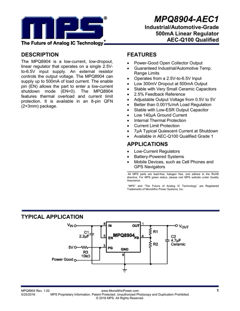
TYPICAL APPLICATION
MPQ8904 Rev. 1.02
www.MonolithicPower.com
5/25/2016
MPS Proprietary Information. Patent Protected. Unauthorized Photocopy and Duplication Prohibited.
© 2016 MPS. All Rights Reserved.
1
MPQ8904 –INDUSTRIAL-GRADE, 500mA LINEAR REGULATOR, AEC-Q100 QUALIFIED
ORDERING INFORMATION
Part Number
MPQ8904DD-AEC1*
MPQ8904DD**
Package
Top Marking
QFN-8 (2mm x 3mm)
See Below
* For Tape & Reel, add suffix –Z (e.g. MPQ8904DD-AEC1–Z);
For RoHS, compliant packaging, add suffix –LF (e.g. MPQ8904DD-AEC1–LF–Z).
** For Tape & Reel, add suffix -Z (e.g. MPQ8904DD-Z);
For RoHS, compliant packaging, add suffix -LF (e.g. MPQ8904DD-LF-Z).
TOP MARKING
T3: product code of MPQ8904DD and MPQ8904DD-AEC1;
Y: year code;
W: week code:
LLL: lot number;
PACKAGE REFERENCE
MPQ8904 Rev. 1.02
www.MonolithicPower.com
5/25/2016
MPS Proprietary Information. Patent Protected. Unauthorized Photocopy and Duplication Prohibited.
© 2016 MPS. All Rights Reserved.
2
MPQ8904 –INDUSTRIAL-GRADE, 500mA LINEAR REGULATOR, AEC-Q100 QUALIFIED
ABSOLUTE MAXIMUM RATINGS (1)
IN, FB to GND ............................... -0.3V to +7V
EN to GND.............................-0.3V to VIN +0.3V
OUT ...................................... -0.3V to VIN + 0.3V
(2)
Continuous Power Dissipation
(TA = +25°C)
……………………………………………….2.5W
Junction Temperature .............................. 150°C
Lead Temperature ................................... 260°C
Storage Temperature .............. -65°C to +150°C
Recommended Operating Conditions
(3)
Input Voltage VIN ............................ 2.5V to 6.5V
Output Voltage .................................. 0.5V to 5V
Load Current.......................... 500mA Maximum
Operating Junction Temp. (TJ). -40°C to +125°C
Thermal Resistance
(4)
θJA
θJC
QFN-8 (2mm x 3mm) .............. 55 ...... 12 ... °C/W
Notes:
1) Exceeding these ratings may damage the device.
2) The maximum allowable power dissipation is a function of the
maximum junction temperature TJ(MAX), the junction-toambient thermal resistance θJA, and the ambient temperature
TA. The maximum allowable continuous power dissipation at
any ambient temperature is calculated by PD(MAX)=(TJ(MAX)TA)/ θJA. Exceeding the maximum allowable power dissipation
will cause excessive die temperature, and the regulator will go
into thermal shutdown. Internal thermal shutdown circuitry
protects the device from permanent damage.
3) The device is not guaranteed to function outside of its
operating conditions.
4) Measured on approximately 1” square of 1 oz copper.
MPQ8904 Rev. 1.02
www.MonolithicPower.com
5/25/2016
MPS Proprietary Information. Patent Protected. Unauthorized Photocopy and Duplication Prohibited.
© 2016 MPS. All Rights Reserved.
3
MPQ8904 –INDUSTRIAL-GRADE, 500mA LINEAR REGULATOR, AEC-Q100 QUALIFIED
ELECTRICAL CHARACTERISTICS
VIN = 3.3V, VOUT = 1.2V, COUT = 4.7µF, CIN = 2.2µF, TJ = -40°C to +125°C, Typical value are TJ =
25°C, unless otherwise noted.
Parameter
Operating Voltage
Ground Pin Current
(7)
Shutdown Current
FB Regulation Voltage
Dropout Voltage
Line Regulation
(8)
(6)
Load Regulation
(6)
Power-Good Output Voltage,
9
Low
Symbol Condition
Min
IOUT = 1mA
2.5
IOUT = 1mA
IOUT = 500mA
VEN = 1.45V, VIN = 5V
TJ = +25°C
0.484
0.478
-40°C TJ +125°C
IOUT = 500mA
200
IOUT
=
1mA,
-0.1
(7)
VIN = (VOUT + 0.5V) to 6.5V
IOUT = 1mA to 500mA,
-0.1
VIN = VOUT + 0.5V
VOL
Isink = 0.5mA
EN Input, High
0
Typ
(4)
140
7
7
0.496
0.496
300
Max
6.5
200
12
15
0.508
0.513
450
Units
V
µA
mA
µA
0.015
0.1
%/V
0.005
0.1
%/mA
0.5
1
V
EN Input, Low
Thermal Protection
Current Limit
VEN = 1.5V
0.05
(5)
650
mV
V
1.2
EN Input Bias Current
V
0.4
V
1
μA
155
°C
850
mA
Notes:
5) Parameter is guaranteed by design, not production tested.
6) Resistors for VOUT measurement are 10kΩ, 14kΩ, 1%
7) The ground current does not include current through feedback current
8) Dropout Voltage is defined as the input to output differential when the output voltage drops 1% below its nominal value
9) VFEEDBACK is 90% of the regulated value with 10kΩ pull-up to 5V
MPQ8904 Rev. 1.02
www.MonolithicPower.com
5/25/2016
MPS Proprietary Information. Patent Protected. Unauthorized Photocopy and Duplication Prohibited.
© 2016 MPS. All Rights Reserved.
4
MPQ8904 –INDUSTRIAL-GRADE, 500mA LINEAR REGULATOR, AEC-Q100 QUALIFIED
TYPICAL PERFORMANCE CHARACTERISTICS
Based on the Figure Typical Application Circuit
C1=2.2μF, C2 =4.7μF, C3=1nF, TA = +25°C, unless otherwise noted.
MPQ8904 Rev. 1.02
www.MonolithicPower.com
5/25/2016
MPS Proprietary Information. Patent Protected. Unauthorized Photocopy and Duplication Prohibited.
© 2016 MPS. All Rights Reserved.
5
MPQ8904 –INDUSTRIAL-GRADE, 500mA LINEAR REGULATOR, AEC-Q100 QUALIFIED
TYPICAL PERFORMANCE CHARACTERISTICS (continued)
C1=2.2μF, C2 =4.7μF, C3=1nF, TA = +25°C, unless otherwise noted.
MPQ8904 Rev. 1.02
www.MonolithicPower.com
5/25/2016
MPS Proprietary Information. Patent Protected. Unauthorized Photocopy and Duplication Prohibited.
© 2016 MPS. All Rights Reserved.
6
MPQ8904 –INDUSTRIAL-GRADE, 500mA LINEAR REGULATOR, AEC-Q100 QUALIFIED
TYPICAL PERFORMANCE CHARACTERISTICS (continued)
C1=2.2μF, C2 =4.7μF, C3=1nF, TA = +25°C, unless otherwise noted.
MPQ8904 Rev. 1.02
www.MonolithicPower.com
5/25/2016
MPS Proprietary Information. Patent Protected. Unauthorized Photocopy and Duplication Prohibited.
© 2016 MPS. All Rights Reserved.
7
MPQ8904 –INDUSTRIAL-GRADE, 500mA LINEAR REGULATOR, AEC-Q100 QUALIFIED
PIN FUNCTIONS
Pin #
Name
1
OUT
2
NC
3
PG
4
FB
5
EN
6
GND
7
NC
No connect.
8
IN
Power Source Input. IN supplies the internal power to the MPQ8904 and is the
source for the pass transistor. Bypass IN to GND with a ≥2.2μF capacitor.
Exposed
Pad
Description
Regulator Output. Bypass OUT to GND with a ≥4.7μF capacitor.
No connect.
Power-Good Open Collector Output. Monitors the regulator output. If the regulator
output falls below 10% of its regulation point, the power-good pin goes low.
Feedback. Connect a resistive voltage divider from OUT to FB to set the output
voltage. OUT feedback threshold is 0.5V.
Enable Input. Drive EN above 1.2V to turn on the MPQ8904. Drive EN below 0.4V to
turn it off.
Ground.
Connect to GND.
OPERATION
The MPQ8904 is a low-current, low-voltage,
low-dropout, linear regulator. It is intended for
devices that require very low voltage and low
quiescent current power, such as wireless
modems and cellular phones.
The MPQ8904 uses a PNP pass element and
features internal thermal shutdown and internal
current limit circuit.
Figure 1: Functional Block Diagram
MPQ8904 Rev. 1.02
www.MonolithicPower.com
5/25/2016
MPS Proprietary Information. Patent Protected. Unauthorized Photocopy and Duplication Prohibited.
© 2016 MPS. All Rights Reserved.
8
MPQ8904 –INDUSTRIAL-GRADE, 500mA LINEAR REGULATOR, AEC-Q100 QUALIFIED
APPLICATION INFORMATION
Setting the Output Voltage
The MPQ8904 has an adjustable output voltage
set via an external resistor divider (R1 and R2
in Figure).
V
VFB
R1 R2 OUT
V
FB
where VFB = 0.5V is the OUT feedback
threshold voltage.
Example: For a 2.5V output and R2=10kΩ
2.5 0.5
R1 10k
40k
0.5
Use a standard 40kΩ (1%) resistor for R1.
Table 1 lists selected R1 values for typical
output voltages (R2 = 10kΩ).
Power-Good
The power-good (PG) pin monitors the output
voltage; if the output voltage goes below 10% of
its regulation point, the PG pin goes low. The
PG pin is an open collector output that connects
to a pull-up resistor (typically 10kΩ). Tie the
pull-up resistor to 0V-to-5.5V supply, such as
regulated input voltage.
Table 1: Adjustable Output Voltage Values vs. R1
(R2 =10kΩ)
VOUT (V)
R1 (Ω)
1.25
15k
1.5
20k
1.8
26k
2
30k
2.5
40k
2.8
46k
3
50k
3.3
56k
4
70k
5
90k
Bypass Capacitors
Bypass the reference voltage can be bypassed
with an external capacitor to reduce noise. Use
a low-ESR ceramic capacitor for the best
performance.
Fast Power On
The MPQ8904 may need an RC circuit to slow
down the fast power on if the power on time is
less than 100μs (see Figure 2). The typical
resistor (R4) value is 100kΩ and the typical
capacitor (C3) value is 10nF.
VIN
8
VIN
VOUT
R1 C3
2.2uF
GND
2
R3
10KΩ
EN
C2
MPQ8904
NC
FB
EN
NC
NC
4
4.7uF
R4
100KΩ
5
C3
10nF
PG
VOUT
1
C1
GND
3
PG
7
R2
GND
6
GND
GND
Figure 2: Fast Power-On Start-Up Circuit
MPQ8904 Rev. 1.02
www.MonolithicPower.com
5/25/2016
MPS Proprietary Information. Patent Protected. Unauthorized Photocopy and Duplication Prohibited.
© 2016 MPS. All Rights Reserved.
9
MPQ8904 –INDUSTRIAL-GRADE, 500mA LINEAR REGULATOR, AEC-Q100 QUALIFIED
TYPICAL APPLICATION CIRCUIT
Figure 3: Typical Application Circuit
MPQ8904 Rev. 1.02
www.MonolithicPower.com
5/25/2016
MPS Proprietary Information. Patent Protected. Unauthorized Photocopy and Duplication Prohibited.
© 2016 MPS. All Rights Reserved.
10
MPQ8904 –INDUSTRIAL-GRADE, 500mA LINEAR REGULATOR, AEC-Q100 QUALIFIED
PCB layout guide
PCB layout is very important to achieve good
regulation, ripple rejection, transient response
and
thermal
performance.
For
optimal
performance, duplicate the EVB layout from
Figure.
For any changes, follow the guidelines below:
1)
Place the input and output ceramic bypass
capacitors close to their respective IN and
OUT pins.
2)
Use short and direct feedback connections.
Place
the
feedback
resistors
and
compensation components as close to the
chip as possible.
3)
Connect IN, OUT and GND to large copper
surfaces to help cool the chip to improve
thermal
performance
and
long-term
reliability.
C2
OUT
IN
R1
R3
R2
C3
OUT
1
8
NC
2
7
NC
PG
3
6
GND
FB
4
5
EN
IN
C1
GND
Figure 4: PCB Layout, Top Layer
MPQ8904 Rev. 1.02
www.MonolithicPower.com
5/25/2016
MPS Proprietary Information. Patent Protected. Unauthorized Photocopy and Duplication Prohibited.
© 2016 MPS. All Rights Reserved.
11
MPQ8904 –INDUSTRIAL-GRADE, 500mA LINEAR REGULATOR, AEC-Q100 QUALIFIED
PACKAGE INFORMATION
QFN-8 (2mm x 3mm)
NOTICE: The information in this document is subject to change without notice. Users should warrant and guarantee that third
party Intellectual Property rights are not infringed upon when integrating MPS products into any application. MPS will not
assume any legal responsibility for any said applications.
MPQ8904 Rev. 1.02
www.MonolithicPower.com
5/25/2016
MPS Proprietary Information. Patent Protected. Unauthorized Photocopy and Duplication Prohibited.
© 2016 MPS. All Rights Reserved.
12


