MPQ8039-AEC1
High Current
Power Half Bridge
AEC-Q100 Qualified
DESCRIPTION
FEATURES
The MPQ8039 is a general purpose, high
frequency half bridge power driver capable of
driving a 9A load. The device integrates both
top and bottom N-Channel MOSFET power
switches and is fully protected from both
sourcing and sinking current by a preset
cycle-by-cycle current limit. It has a wide input
voltage range from 7.5V to 25V.
•
The MPQ8039 features a low-current shutdown
mode, input under-voltage protection, thermal
shutdown. It interfaces with standard logic
signals and is available in a small SOIC8E
package.
•
•
•
•
•
•
•
•
•
•
•
Guaranteed Industrial/Automotive Temp.
Range Limits
±9A Peak Current Output
±4.25A Continuous Current Output
Up to 1.2MHz Switching Frequency
Protected Integrated Power 100mΩ Switches
All Switches Current Limited
Integrated Under-Voltage Protection
Integrated Thermal Protection
2.5μA Standby Mode
True 2-Quadrant Operation
Sources and Sinks Current
Available in AEC-Q100 Qualified Grade
APPLICATIONS
•
•
•
Class D Audio Driver
o 25W/4Ω/10% Output Power Single Ended
o 70W/4Ω/10% Output Power Full Bridge
Full or Half Bridge DC-DC Switching Regulator
Motor Driver
All MPS parts are lead-free and adhere to the RoHS directive. For MPS green
status, please visit MPS website under Products, Quality Assurance page.
“MPS” and “The Future of Analog IC Technology” are Trademarks of
Monolithic Power Systems, Inc.
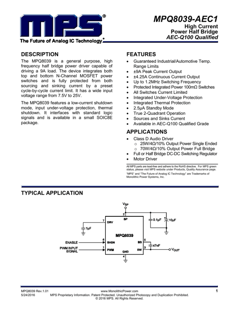
TYPICAL APPLICATION
MPQ8039 Rev.1.01
www.MonolithicPower.com
5/24/2016
MPS Proprietary Information. Patent Protected. Unauthorized Photocopy and Duplication Prohibited.
© 2016 MPS. All Rights Reserved.
1
MPQ8039 – HIGH CURRENT POWER HALF BRIGDE, AEC-Q100 QUALIFIED
ORDERING INFORMATION
Part Number
MPQ8039GN*
MPQ8039GN-AEC1**
Package
SOIC8E
SOIC8E
Top Marking
MP8039
MP8039
* For Tape & Reel, add suffix –Z (eg. MPQ8039GN–Z)
** For Tape & Reel, add suffix –Z (eg. MPQ8039GN-AEC1–Z)
PACKAGE REFERENCE
ABSOLUTE MAXIMUM RATINGS (1)
SP Supply Voltage (VSP) .............. -0.3V to +28V
SW Pin Voltage...............................–0.3V to VSP
SW to BS .......................................–0.3V to +6V
Voltage at All Other Pins ................–0.3V to +6V
(2)
Continuous Power Dissipation (TA = +25°C)
............................................................2.5W
Storage Temperature .............. –55°C to +150°C
Recommended Operating Conditions
(3)
SP Supply Voltage (VSP) ................. 7.5V to 24V
Peak Output Current ..................... 9A Maximum
Operating Junction Temp. (TJ). -40°C to +125°C
Thermal Resistance
(4)
θJA
θJC
SOIC8E .................................. 48 ...... 10 ... °C/W
Notes:
1) Absolute maximum ratings are rated under room temperature
unless otherwise noted. Exceeding these ratings may
damage the device.
2) The maximum allowable power dissipation is a function of the
maximum junction temperature TJ (MAX), the junction-toambient thermal resistance θJA, and the ambient temperature
TA. The maximum allowable continuous power dissipation at
any ambient temperature is calculated by PD (MAX) = (TJ
(MAX)-TA)/θJA. Exceeding the maximum allowable power
dissipation will cause excessive die temperature, and the
regulator will go into thermal shutdown. Internal thermal
shutdown circuitry protects the device from permanent
damage.
3) The device is not guaranteed to function outside of its
operating conditions.
4) Measured on approximately 1” square of 1 oz copper.
MPQ8039 Rev.1.01
www.MonolithicPower.com
5/24/2016
MPS Proprietary Information. Patent Protected. Unauthorized Photocopy and Duplication Prohibited.
© 2016 MPS. All Rights Reserved.
2
MPQ8039 – HIGH CURRENT POWER HALF BRIGDE, AEC-Q100 QUALIFIED
ELECTRICAL CHARACTERISTICS
VSP = 12V, VSHDN = 0V, TJ = -40°C to +125°C, Typical value are TJ = 25°C, unless otherwise noted.
Parameter
SP Operating Current
SP Shutdown Current
SHDN, SP Threshold Low
SHDN, SP Threshold High
SHDN, SP Input Bias Current
SW On Resistance
SW Current Limit
Symbol Condition
VSHDN = 2V
VSP = 7.5V, High-Side and Low-Side
VPWM = 5, (Sinking)
VPWM = 0, (Sourcing)
VPWM = 0 to 2V, 50% Duty Cycle
VSP = 7.5V, VPWM = 2V, CSW 100nF,
fSW = 3.3kHz
VPWM = 0 to 5V
VPWM = 0 to 2V, High or Low Pulse
VPWM = 0 to 5V
SW Switching Frequency
(6)
SW Rise/Fall Time
PWM Pulse Width
PWM to SW Delay Time Rising
PWM to SW Delay Time
Falling
Thermal Shutdown
(5)
Temperature
IN UVLO
DRV Voltage
PWM Threshold Voltage
Typ
1.5
2.5
Max
2.5
10
1
2
(5)
SW Maximum Duty Cycle
Min
VDRV
1
0.1
9
9
0.25
1.2
Units
mA
μA
V
V
μA
Ω
A
A
MHz
99.5
%
20
70
ns
ns
ns
VPWM = 5 to 0V
70
ns
TJ Rising, Hysteresis = 20°C
160
°C
Rising Edge
VSP=10V
VPWM Rising
VPWM Falling
200
5.5
5.1
5.6
1.3
7.5
6.0
2.4
V
V
V
V
Notes:
5) Not production tested.
6) SW drives low for 1.5μs every 300μs to charge the BS to SW capacitor.
MPQ8039 Rev.1.01
www.MonolithicPower.com
5/24/2016
MPS Proprietary Information. Patent Protected. Unauthorized Photocopy and Duplication Prohibited.
© 2016 MPS. All Rights Reserved.
3
MPQ8039 – HIGH CURRENT POWER HALF BRIGDE, AEC-Q100 QUALIFIED
TYPICAL PERFORMANCE CHARACTERISTICS
Circuit of Figure 4, TA = +25°C, unless otherwise noted.
MPQ8039 Rev.1.01
www.MonolithicPower.com
5/24/2016
MPS Proprietary Information. Patent Protected. Unauthorized Photocopy and Duplication Prohibited.
© 2016 MPS. All Rights Reserved.
4
MPQ8039 – HIGH CURRENT POWER HALF BRIGDE, AEC-Q100 QUALIFIED
TYPICAL PERFORMANCE CHARACTERISTICS
VIN=24V, RLOAD=4Ω, L=10uH, FIN=0.5MHz, TA=25ºC, Unless otherwise noted.
MPQ8039 Rev.1.01
www.MonolithicPower.com
5/24/2016
MPS Proprietary Information. Patent Protected. Unauthorized Photocopy and Duplication Prohibited.
© 2016 MPS. All Rights Reserved.
5
MPQ8039 – HIGH CURRENT POWER HALF BRIGDE, AEC-Q100 QUALIFIED
PIN FUNCTIONS
Pin #
Name
1
PWM
2
SP
3
SW
4
GND
5
BS
6
SHDN
7
DRV
8
N/C
Description
Driver Logic Input. Drive PWM with the signal that controls the MPQ8039 output. Drive
PWM high to turn on the high-side switch; drive PWM low to turn on the low-side switch.
Power Supply Input. Connect SP to the positive side of the input power supply. Bypass SP
to GND as close to the IC as possible.
Switched Output. SW is the power output of the MPQ8039. Connect the output LC filter to
SW. SW is valid approximately 100μs after SP goes high.
Ground. (Note: Connect the exposed pad on the bottom side to Pin 4).
Bootstrap Supply. BS powers the high-side gate of the MPQ8039. Connect a 0.1μF or
greater capacitor between BS and SW.
Shutdown Input. SHDN enables/disables the MPQ8039. Drive SHDN low to turn on the
MPQ8039, drive it high to turn it off. If not used, connect SHDN to GND.
Gate Drive Supply Bypass. The voltage at DRV is supplied from an internal regulator from
SP. DRV powers the internal circuitry and internal MOSFET gate drives. Bypass DRV to
GND with a 0.1μF to 10μF capacitor.
MPQ8039 Rev.1.01
www.MonolithicPower.com
5/24/2016
MPS Proprietary Information. Patent Protected. Unauthorized Photocopy and Duplication Prohibited.
© 2016 MPS. All Rights Reserved.
6
MPQ8039 – HIGH CURRENT POWER HALF BRIGDE, AEC-Q100 QUALIFIED
OPERATION
The MPQ8039 is a general purpose, power
driver. It takes a logic input and drives a half
bridge comprised of 0.1Ω high-side and
low-side N-Channel MOSFET switches.
It operates at frequencies up to 1.2MHz, can
accept a DC supply voltage as high as 25V,
and produce peak output current as high as 9A.
Figure 1: Function Block Diagram
SW Output
The SW output drives the load. It is controlled
by the logic input signal at PWM. When the
signal at PWM is high (above 2V), the high-side
switch is turned on. When the signal at PWM is
low (less than 0.4V), the low-side switch is
turned on.
The MPQ8039 uses internal N-Channel
MOSFETs for both the high-side and low-side
switches. The high-side MOSFET gate drive is
powered from the voltage between SW and BS,
allowing BS to rise above the SP input voltage
to power the high-side MOSFET. To do this a
bootstrap capacitor is connected between SW
and BS. When the low-side switch is on, the
capacitor is internally charged from the voltage
at DRV, which is also internally generated.
There is a dead time region (typically 40ns)
where both the upper and lower switches are
off (see Figure 2).
Both the high-side and low-side switches have
internal current limits to prevent failure due to
excessive load current. Once the current limit is
reached, both output switches are turned off
and the fault output is asserted (driven low).
Shutdown
The MPQ8039 includes a 2.5μA shutdown
mode. When SHDN is high, both output
switches are turned off and the input current
drops to 2.5μA. When the MPQ8039 is
shutdown, the internally generated voltage at
DRV drops to 0V. If the shutdown mode is not
used, connect SHDN directly to GND.
MPQ8039 Rev.1.01
www.MonolithicPower.com
5/24/2016
MPS Proprietary Information. Patent Protected. Unauthorized Photocopy and Duplication Prohibited.
© 2016 MPS. All Rights Reserved.
7
MPQ8039 – HIGH CURRENT POWER HALF BRIGDE, AEC-Q100 QUALIFIED
Thermal Shutdown
The MPQ8039 includes a thermal overload
protection circuit. If the die temperature rises
above 160°C, the output switches are turned off
and the fault output is asserted. Once the
thermal overload circuit is tripped, the die
temperature must drop below 140°C before
automatically restarting.
Figure 2: Dead Time
MPQ8039 Rev.1.01
www.MonolithicPower.com
5/24/2016
MPS Proprietary Information. Patent Protected. Unauthorized Photocopy and Duplication Prohibited.
© 2016 MPS. All Rights Reserved.
8
MPQ8039 – HIGH CURRENT POWER HALF BRIGDE, AEC-Q100 QUALIFIED
TYPICAL APPLICATION CIRCUITS
Figure 3: Single Ended Audio Amplifier
Figure 4: General Purpose DC to DC
Converter
Figure 5: 80W Full Bridge Audio Amplifier
Figure 6: Full Bridge Motor Driver
MPQ8039 Rev.1.01
www.MonolithicPower.com
5/24/2016
MPS Proprietary Information. Patent Protected. Unauthorized Photocopy and Duplication Prohibited.
© 2016 MPS. All Rights Reserved.
9
MPQ8039 – HIGH CURRENT POWER HALF BRIGDE, AEC-Q100 QUALIFIED
Figure 7: CCFL Driver Circuit
MPQ8039 Rev.1.01
www.MonolithicPower.com
5/24/2016
MPS Proprietary Information. Patent Protected. Unauthorized Photocopy and Duplication Prohibited.
© 2016 MPS. All Rights Reserved.
10
MPQ8039 – HIGH CURRENT POWER HALF BRIGDE, AEC-Q100 QUALIFIED
PACKAGE INFORMATION
SOIC8N (EXPOSED PAD)
NOTICE: The information in this document is subject to change without notice. Please contact MPS for current specifications.
Users should warrant and guarantee that third party Intellectual Property rights are not infringed upon when integrating MPS
products into any application. MPS will not assume any legal responsibility for any said applications.
MPQ8039 Rev. 1.01
www.MonolithicPower.com
5/24/2016
MPS Proprietary Information. Patent Protected. Unauthorized Photocopy and Duplication Prohibited.
© 2016 MPS. All Rights Reserved.
11
Mouser Electronics
Authorized Distributor
Click to View Pricing, Inventory, Delivery & Lifecycle Information:
Monolithic Power Systems (MPS):
MPQ8039GN MPQ8039GN-Z


