Evaluation Board for Wideband
CMOS 4:1 Mux/SP4T
EVAL-ADG904/ADG904-R
FEATURES
EN
GND VDD
J12
1
Evaluation board for the ADG904/ADG904-R
RF through for evaluation board calibration
A1
J1
H
L
C1
INTRODUCTION
A0
J3
K1
J2
H
L
H
L
K3
K2
J6
J5
This evaluation board document describes the evaluation board
for the ADG904/ADG904-R wideband multiplexers.
RF2
RF1
C2 C3
U1
The ADG904/ADG904-R are wideband, analog 4:1 multiplexers,
using a CMOS process to provide high isolation and low insertion loss to 1 GHz. The ADG904 is an absorptive/matched mux
having 50 Ω terminated shunt legs, whereas the ADG904-R is a
reflective mux. These devices are designed such that the isolation
is high over the dc to1 GHz frequency range.
J8
J7
RF4
RF3
EVAL-ADG904-R/ADG904
J4
J10
RFC
CAL
06280-001
CAL
J9
The ADG904/ADG904-R switch one of four inputs to a
common output, RFC, as determined by the 3-bit binary
address lines (A0, A1, and EN). A Logic 1 on the EN pin
disables the device.
The ADG904/ADG904-R have on-board CMOS control logic,
thus eliminating the need for external controlling circuitry. The
control inputs are CMOS compatible.
Complete information and specifications for the ADG904 and
ADG904-R are available in the ADG904/ADG904-R data sheet
available from Analog Devices, Inc., and should be consulted in
conjunction with this evaluation board document when using
the evaluation board.
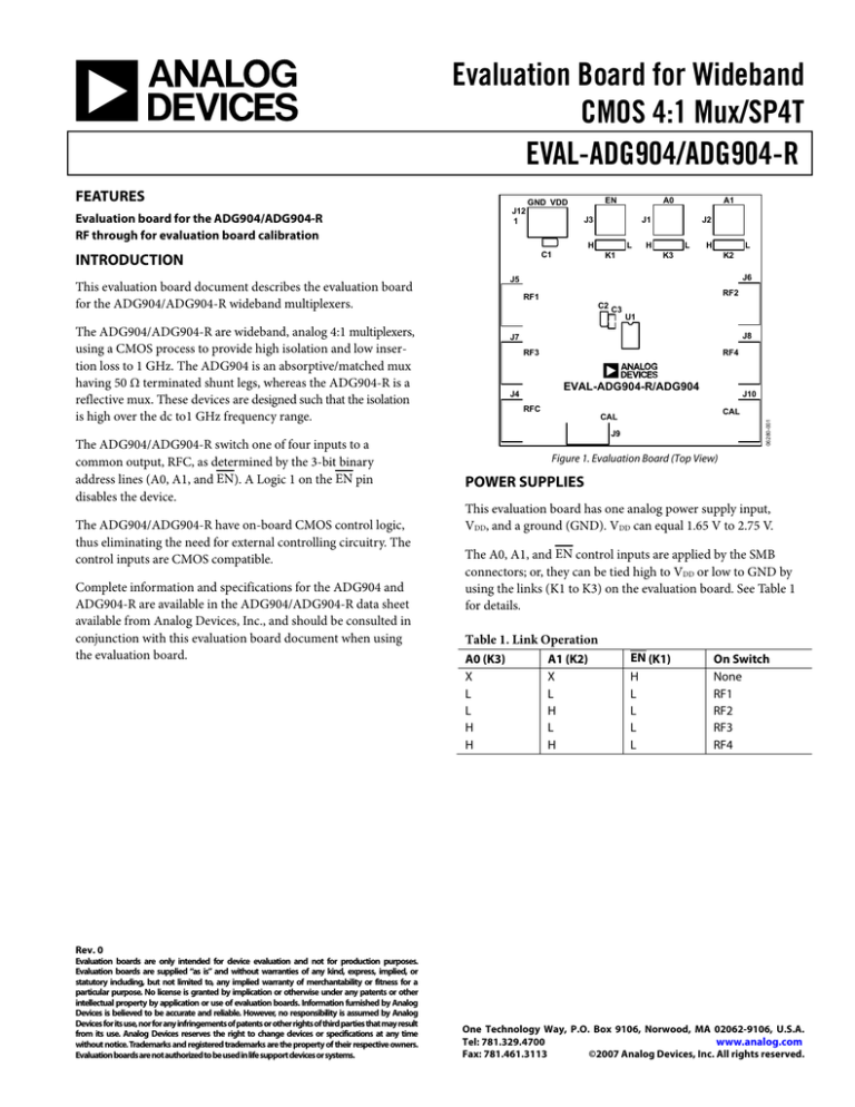
Figure 1. Evaluation Board (Top View)
POWER SUPPLIES
This evaluation board has one analog power supply input,
VDD, and a ground (GND). VDD can equal 1.65 V to 2.75 V.
The A0, A1, and EN control inputs are applied by the SMB
connectors; or, they can be tied high to VDD or low to GND by
using the links (K1 to K3) on the evaluation board. See Table 1
for details.
Table 1. Link Operation
A0 (K3)
X
L
L
H
H
A1 (K2)
X
L
H
L
H
EN (K1)
H
L
L
L
L
On Switch
None
RF1
RF2
RF3
RF4
Rev. 0
Evaluation boards are only intended for device evaluation and not for production purposes.
Evaluation boards are supplied “as is” and without warranties of any kind, express, implied, or
statutory including, but not limited to, any implied warranty of merchantability or fitness for a
particular purpose. No license is granted by implication or otherwise under any patents or other
intellectual property by application or use of evaluation boards. Information furnished by Analog
Devices is believed to be accurate and reliable. However, no responsibility is assumed by Analog
Devices for its use, nor for any infringements of patents or other rights of third parties that may result
from its use. Analog Devices reserves the right to change devices or specifications at any time
without notice. Trademarks and registered trademarks are the property of their respective owners.
Evaluation boards are not authorized to be used in life support devices or systems.
One Technology Way, P.O. Box 9106, Norwood, MA 02062-9106, U.S.A.
www.analog.com
Tel: 781.329.4700
Fax: 781.461.3113
©2007 Analog Devices, Inc. All rights reserved.
EVAL-ADG904/ADG904-R
TABLE OF CONTENTS
Features .............................................................................................. 1 Schematic ............................................................................................4 Introduction ...................................................................................... 1 Ordering Information .......................................................................5 Power Supplies .................................................................................. 1 Bill of Materials ..............................................................................5 Revision History ............................................................................... 2 Ordering Guide .............................................................................5 ADG904/ADG904-R ....................................................................... 3 ESD Caution...................................................................................5 REVISION HISTORY
9/07—Revision 0: Initial Version
Rev. 0 | Page 2 of 8
EVAL-ADG904/ADG904-R
ADG904/ADG904-R
Two 10 μF surface-mount, tantalum decoupling capacitors are
provided on the VDD line, one placed close to the DUT along
with a 100 pF ceramic capacitor on the VDD line.
The RFC port is connected through a 50 Ω transmission line to
the bottom left SMA Connector J4. RF1, RF2, RF3, and RF4 are
connected through 50 Ω transmission lines to the SMA connectors
(J5, J6, J7, and J8, respectively). A through transmission line
connects J9 and J10, and this transmission line is used to estimate
the loss of the PCB over the environmental conditions being
evaluated (see Figure 2).
EN
GND VDD
J12
1
A0
J3
J1
H
C1
A1
L
K1
J2
H
L
K3
Rev. 0 | Page 3 of 8
L
K2
J6
J5
RF2
RF1
C2 C3
U1
J8
J7
RF4
RF3
The board is constructed of a 4-layer, FR4 material with a
dielectric constant of 4.3 and an overall thickness of 0.062 inches.
Two ground layers with grounded planes provide ground for
the RF transmission lines. The design of the transmission lines
incorporates a coplanar wave guide with a ground plane model
using a trace width of 0.024 inches, clearance to a ground plane
of 0.008 inches, dielectric thickness of 0.02 inches, and a metal
thickness of 0.0021 inches.
H
EVAL-ADG904-R/ADG904
J4
RFC
CAL
J10
CAL
J9
Figure 2. ADG904/ADG904-R Evaluation Board (Top View)
06280-001
The ADG904/ADG904-R evaluation board allows designers to
evaluate the high performance, wideband switches with
minimum effort. To test these devices to ensure that they meet
the user’s requirements, the user needs only a power supply and
a network analyzer to use this evaluation board.
EVAL-ADG904/ADG904-R
SCHEMATIC
J9
J10
CAL
RF1
J4
RF2
RFC
10
ADG904/
ADG904-R
U1
J1
20 A0
J2
19
J3
1
VDD
+ C1
VDD
2
+ C2
RF1
17
RF2
7
RF3
RFC
RF3
J12-1
4
A1
EN
VDD
RF4 14
GND
GND
GND
GND
GND
GND
GND
GND
GND
GND
GND
RF4
J5
J6
J7
J8
3
5
6
8
9
11
12
13
15
16
18
C3
100pF
J12-2
B
A
K1
B
A
K2
B
K3
06280-002
A
Figure 3. Schematic of the ADG904/ADG904-R Evaluation Board
Rev. 0 | Page 4 of 8
EVAL-ADG904/ADG904-R
ORDERING INFORMATION
BILL OF MATERIALS
Table 2. Bill of Materials
Item
1
2
3
4
5
6
7
Quantity
2
1
3
7
1
3
1
Reference
C1, C2
C3
J1, J2, J3
J4 to J10
J12
K1, K2, K3
U1
Part Description
10 μF, 10 V tantalum capacitor
100 pF NPO ceramic capacitor
Straight SMB jack
SMA end-launch RF connector
2-pin terminal block
JUMPER2/SIP3
ADG904-R/ADG904
ORDERING GUIDE
Model
EVAL-ADG904EBZ1
EVAL-ADG904REB
1
Supplier/No.
FEC 197-130
FEC 722-080
FEC 310-682
Johnson Components 142-0701-851
FEC 151-785
FEC 512-047 and FEC 150-410
Analog Devices, Inc.
ESD CAUTION
Description
Evaluation Board
Evaluation Board
Z = RoHS Compliant Part.
Rev. 0 | Page 5 of 8
EVAL-ADG904/ADG904-R
NOTES
Rev. 0 | Page 6 of 8
EVAL-ADG904/ADG904-R
NOTES
Rev. 0 | Page 7 of 8
EVAL-ADG904/ADG904-R
NOTES
©2007 Analog Devices, Inc. All rights reserved. Trademarks and
registered trademarks are the property of their respective owners.
EB06280-0-9/07(0)
Rev. 0 | Page 8 of 8
Mouser Electronics
Authorized Distributor
Click to View Pricing, Inventory, Delivery & Lifecycle Information:
Analog Devices Inc.:
EVAL-ADG904EBZ EVAL-ADG904REBZ
