Lecture 30: Biasing MOSFET Amplifiers. MOSFET Current Mirrors.
advertisement
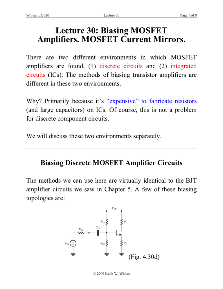
Whites, EE 320 Lecture 30 Page 1 of 8 Lecture 30: Biasing MOSFET Amplifiers. MOSFET Current Mirrors. There are two different environments in which MOSFET amplifiers are found, (1) discrete circuits and (2) integrated circuits (ICs). The methods of biasing transistor amplifiers are different in these two environments. Why? Primarily because it’s “expensive” to fabricate resistors (and large capacitors) on ICs. Of course, this is not a problem for discrete component circuits. We will discuss these two environments separately. Biasing Discrete MOSFET Amplifier Circuits The methods we can use here are virtually identical to the BJT amplifier circuits we saw in Chapter 5. A few of these biasing topologies are: (Fig. 4.30d) © 2009 Keith W. Whites Whites, EE 320 Lecture 30 (Fig. 4.32) Page 2 of 8 (Fig. 4.33a) Example N30.1. Design the MOSFET amplifier below so that I D = 1 mA and allow for a drain voltage swing of ±2 V. The amplifier is to present a 1-MΩ input resistance to a capacitively coupled input signal. The transistor has kn′ W L = 0.5 mA/V2 and Vt = 2 V. I D = 1 mA ∞ ∞ vi vo Whites, EE 320 Lecture 30 Page 3 of 8 We can see directly from this circuit that at DC, VG = 0 . Recall that for operation in the saturation mode VGD ≤ Vt (with VGS > 0 ). Now, for ±2 -V swing in vo and large AC gain, we want RD to be large. Hence, let’s choose VD = 0 (since Vt = 2 V). Then for this ±2 -V swing in vo VGD min = 0 − 2 = −2 V < Vt and VGD max = 0 + 2 = 2 V = Vt Because of these results, the MOSFET stays in saturation. Consequently, with VD = 0 V − VD 10 − 0 RD = DD = = 10 kΩ 1 mA 1 mA For a saturated MOSFET 1 W 2 2 I D = kn′ (VGS − Vt ) = 0.25 × 10⁻³ (VGS − 2 ) 2 L For I D = 1 mA ⇒ (VGS − 2) 2 = 4 or VGS = ±2 + 2 = +4 V or 0 V. With VG = 0 and VGS = 4 V then VS = −4 V. Hence, −4 − ( −10 ) = 6 kΩ RS = 1 mA Lastly, for a 1-MΩ AC input resistance, then referring to the input portion of the small-signal model Whites, EE 320 Lecture 30 vgs Page 4 of 8 g m vgs vo we see that Rin = RG ⇒ RG = 1 MΩ Biasing IC MOSFET Amplifiers. Current Mirrors. For MOSFET amplifier biasing in ICs, DC current sources are usually used. As discussed in Lecture 17, “golden currents” are produced using sophisticated multi-component circuits. Then current mirroring (aka current steering) circuits are used to replicate this golden current to provide DC biasing currents at different points in the IC. The basic MOSFET current mirror is shown in Fig. 4.33b for NMOS. (This is basically the same circuit we saw with the BJT current mirror in Lecture 17.) Whites, EE 320 Lecture 30 Page 5 of 8 (Fig. 4.33b) Q1 has the drain and gate terminals connected together. This forces Q1 to operate in the saturation mode in this particular circuit if I D1 ≠ 0 . In this mode 1 W 2 I D1 = kn1′ 1 (VGS − Vt1 ) (4.50),(1) 2 L1 With a zero gate current, I REF = I D1 (2) where we can easily see from the above circuit that V − V − ( −VSS ) I REF = DD GS (4.51),(3) R Now, we’ll assume the two MOSFETs in the circuit have the same VGS. Consequently, the drain current in the second transistor is 1 W 2 I D 2 = kn 2′ 2 (VGS − Vt 2 ) (4) 2 L2 Whites, EE 320 Lecture 30 Page 6 of 8 If these two transistors are perfectly matched but perhaps fabricated with different channel dimensions, then kn1′ = kn 2′ , and Vt1 = Vt 2 so that we see by comparing (1) and (4) that W L W L I D 2 = 2 2 I D1 = 2 2 I REF (4.53),(5) W1 L1 W1 L1 In this NMOS current mirror shown above, Q2 acts as a current sink since it pulls current I O = I D 2 from the load, which is the amplifier circuit of Fig. 4.33a in this case. In PMOS this current mirror circuit is constructed as VDD Q2 Q1 ≈0 IO = I D 2 R I REF To amplifier circuit Here Q2 acts as a current source since it pushes current I O = I D 2 into the load. Example N30.2. Design an NMOS current mirror with VDD = 5 V, VSS = 0, and I REF = 100 μA. For the matched transistors L = 10 μm, W = 100 μm, Vt = 1 V, and kn′ = 20 μA/V2. Whites, EE 320 Lecture 30 Page 7 of 8 Referring to the NMOS current mirror circuit in Fig. 4.33b above, notice that the drain of Q1 is connected to its gate so that VGD1 = 0 , which is less than Vt. This means Q1 is operating in the saturation mode (or is possibly cutoff). Assuming operation in saturation, 1 W 2 I D1 = I REF = kn′ (VGS − Vt ) L 2 1 100 2 = ⋅ 20 × 10−6 ⋅ ⋅ (VGS − 1) 2 10 For I REF = 100 μA ⇒ 100 = 10 ⋅10 (VGS − 1) or VGS = ±1 + 1 = 2 V or 0 V 2 Now, by KVL VDD = I REF R + VGS With VGS = 2 V then R= 5−2 VDD − VGS = = 30 kΩ 100 μA I REF Here are a few additional questions based on this design: • What is the lowest possible value for VO = VD 2 and still have a functioning current mirror? As with Q1, the transistor Q2 must also operate in saturation if it’s going to supply a constant current. Whites, EE 320 Hence Therefore, Lecture 30 Page 8 of 8 VGD 2 ≤ Vt ⇒ VG 2 − VD 2 ≤ Vt ∴ VO = VD 2 ≥ VG 2 − Vt or VO ≥ VGS − Vt = 2 − 1 = 1 V VO min = 1 V • Imagine that VA = 107 L . (Notice that VA is proportional to the channel length, which is commonplace.) What is ro? VA = 107 ⋅10 × 10−6 = 100 V V 100 V ro = A = = 1 MΩ I O 100 μA • What is change in the output current IO if VO changes by 3 V? ΔV 3V = 3 μA ΔIO = O = ro 1 MΩ

