Concerning the packages for Integrated Circuits
Thermal resistance
and thermal characterization parameter
No.AEA-0003 E
Contents
1.Scope ・・・・・・・・・・・・・・・・・・・・・・・・・・・・・・・・・・・・ 1
2.Normative references
・・・・・・・・・・・・・・・・・・・・・・・・・・・・・ 1
3.Terms and definitions
・・・・・・・・・・・・・・・・・・・・・・・・・・・・・ 1,2
4.Test method environmental conditions
5.Test board
・・・・・・・・・・・・・・・・・・・・・・ 2
・・・・・・・・・・・・・・・・・・・・・・・・・・・・・・・・・・ 3
6.Thermal measurement procedure
・・・・・・・・・・・・・・・・・・・・・・・・ 4
1. Scope
The definition and how to use thermal resistance and thermal characterization parameter of packages for ROHM’s
integrated circuit are described in this application note.
2. Normative references
The contents that has been described in this application note complies with JESD51-2A,3,5,7,9,10(JEDEC).
3. Terms and definitions
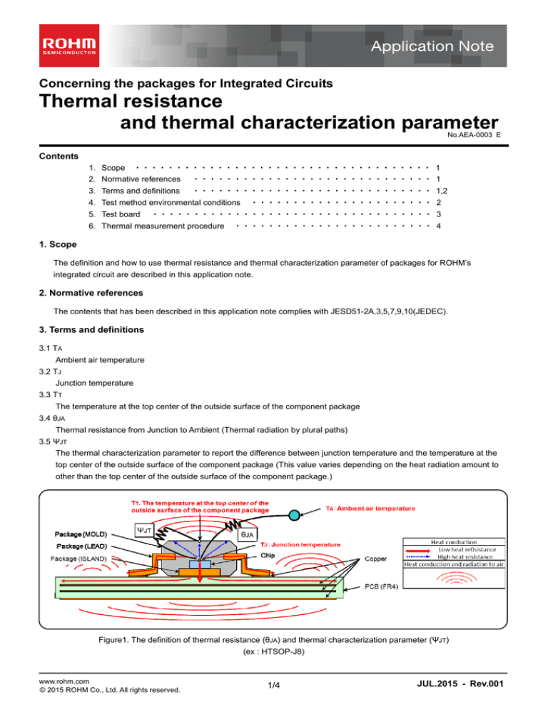
3.1 TA
Ambient air temperature
3.2 TJ
Junction temperature
3.3 TT
The temperature at the top center of the outside surface of the component package
3.4 θJA
Thermal resistance from Junction to Ambient (Thermal radiation by plural paths)
3.5 ΨJT
The thermal characterization parameter to report the difference between junction temperature and the temperature at the
top center of the outside surface of the component package (This value varies depending on the heat radiation amount to
other than the top center of the outside surface of the component package.)
Figure1. The definition of thermal resistance (θJA) and thermal characterization parameter (ΨJT)
(ex : HTSOP-J8)
www.rohm.com
© 2015 ROHM Co., Ltd. All rights reserved.
1/4
JUL.2015 - Rev.001
Thermal resistance and Thermal characterization parameter
Application Note
Figure2. Data sheet example (ex : HTSOP-J8)
4. Test method environmental conditions(JESD51-2A)
Thermal test method environmental conditions comply with JESD51-2A (Still-Air) as below.
Figure3. Thermal test method environmental conditions
Table1. Measurement equipment for thermal resistance
Measurement equipment
Supplier
Type
Note
Thermal tester
Mentor Graphics
T3Ster
for thermal characterization
Thermostat
Mentor Graphics
T3Ster
Thermocouple(NOTE1)
SAKAGUCHI E.H VOC CORP.
K6010
Class1 / Φ0.1mm
(NOTE1) By fixing the thermocouple to the top center of the outside surface of the component package, the temperature at the
top center of the outside surface of the component package is measured.
www.rohm.com
© 2015 ROHM Co., Ltd. All rights reserved.
2/4
JUL.2015 - Rev.001
Application Note
Thermal resistance and Thermal characterization parameter
5. Test board
Thermal test board complies with JESD51-3,5,7,9,10 as below.
Table2. Specified parameters and values used for PCB design. (PKG size is specified by a maximum body length.)
(NOTE1)
Layer
SMD
(PKG size<27mm)
BGA,THD
(PKG size≦40mm)
1s
2s2p
1s
2s2p
Layer
SMD
(PKG size<27mm)
BGA,THD
(PKG size≦40mm)
1s
2s2p
1s
2s2p
Material
Board Size
FR-4
114.3mm x 76.2mm x 1.57mmt
114.3mm x 76.2mm x 1.6mmt
FR-4
114.5mm x 101.5mm x 1.6mmt
Component trace
Copper pattern
Thickness
Component mounting
70µm
and trace fan-out region
Component mounting
70µm
and trace fan-out region
Thermal via
Pitch
Diameter
1.20mm Φ0.30mm
1.20mm Φ0.30mm
Plane
Copper pattern
2
74.2mm (Square)
2
99.5mm ( Square )
Through-hole via
Diameter
Φ0.85mm
Φ0.85mm
Thickness
35µm
35µm
(NOTE2)
Backside trace
Copper pattern
Thickness
2
74.2mm ( Square )
70µm
2
99.5mm ( Square )
70µm
(NOTE1) Thermal via : One thermal via will exist for each trace square of a thermal attach area for a universal test board design.
Thermal vias are designed on the thermal attach pad.(Only the package with heatsink)
(NOTE2) Through-hole via : Pins that are directly connected to the die pad shall be connected to the top buried copper plane.
These pins shall be isolated from the bottom copper plane.
Figure4. Sectional view of the thermal test board (SMD with heat sink)
Figure5. Sectional view of the thermal test board (THD : DIP type)
www.rohm.com
© 2015 ROHM Co., Ltd. All rights reserved.
3/4
JUL.2015 - Rev.001
Application Note
Thermal resistance and Thermal characterization parameter
6. Thermal measurement procedure
Below are two methods of thermal measurement for semiconductor;
-Thermal measurement at the surface of the package (connected measurement / unconnected measurement)
-Thermal measurement at the PN junction of the chip
The advantages and disadvantages of each method are written in the table below;
Table3. The advantages and disadvantages due to differences in measurement method
Measurement method
Advantages
Disadvantage
It is likely to contain some errors due to
Thermal measurement at the
Measurement is easy.
environment because it is not directly
surface of the package
monitored.
Thermal measurement at the
PN junction of the chip
Junction temperature is directly
measured, resulting in a good accuracy.
The terminal for thermal measurement is
needed for semiconductor.
Thermocouple ultrafine
Thermal measurement
Thermal measurement
Thermal measurement
at the surface
at the surface
at the PN junction of the chip
Thermocouple (Connected)
Thermoviewer (Unconnected)
Figure6. Images of each measurement
If surface temperature measurement is used in performing the semiconductor temperature measurement, thermal
characterization parameter (ΨJT) will be used for the calculation.
(ΨJT) is a parameter which defines the temperature difference between junction temperature (TJ) and the temperature at
the top center of the outside surface of the component package (TT), and it is same as ROHM previously used notation (θJC).
An accurate junction temperature can be calculated by using thermal characterization parameter if temperature (TT) is
measured while the thermalcouple is firmly contacted with the top center of the package.
(However, it must be considered that thermal characterization parameter changes depending on heat dissipation performance
of the board.)
TJ = TT + ΨJT ⋇ P
(TJ : Junction temperature , TT : the temperature at the top center of the outside surface of the component package ,
P : Power consumption)
In addition, junction temperature can be easily calculated by using thermal resistance (θJA).
(However, it is likely to be influenced by the difference with JEDEC environment rather than thermal characterization parameter)
TJ = TA + θJA ⋇ P
(TJ : Junction temperature , TA : Ambient temperature , P : Power consumption)
In case of checking the margin to the temperature limit from the package surface temperature, by assuming that TC=TT,
maximum temperature (TCMAX) at the top surface of the component package can be calculated as below.
TCMAX = TJMAX - ΨJT ⋇ P
(TCMAX : Maximum temperature at the top surface of the component package , TJMAX : Maximum junction temperature ,
P : Power consumption)
www.rohm.com
© 2015 ROHM Co., Ltd. All rights reserved.
4/4
JUL.2015 - Rev.001
Notice
Notes
1) The information contained herein is subject to change without notice.
2) Before you use our Products, please contact our sales representative and verify the latest specifications :
3) Although ROHM is continuously working to improve product reliability and quality, semiconductors can break down and malfunction due to various factors.
Therefore, in order to prevent personal injury or fire arising from failure, please take safety
measures such as complying with the derating characteristics, implementing redundant and
fire prevention designs, and utilizing backups and fail-safe procedures. ROHM shall have no
responsibility for any damages arising out of the use of our Poducts beyond the rating specified by
ROHM.
4) Examples of application circuits, circuit constants and any other information contained herein are
provided only to illustrate the standard usage and operations of the Products. The peripheral
conditions must be taken into account when designing circuits for mass production.
5) The technical information specified herein is intended only to show the typical functions of and
examples of application circuits for the Products. ROHM does not grant you, explicitly or implicitly,
any license to use or exercise intellectual property or other rights held by ROHM or any other
parties. ROHM shall have no responsibility whatsoever for any dispute arising out of the use of
such technical information.
6) The Products are intended for use in general electronic equipment (i.e. AV/OA devices, communication, consumer systems, gaming/entertainment sets) as well as the applications indicated in
this document.
7) The Products specified in this document are not designed to be radiation tolerant.
8) For use of our Products in applications requiring a high degree of reliability (as exemplified
below), please contact and consult with a ROHM representative : transportation equipment (i.e.
cars, ships, trains), primary communication equipment, traffic lights, fire/crime prevention, safety
equipment, medical systems, servers, solar cells, and power transmission systems.
9) Do not use our Products in applications requiring extremely high reliability, such as aerospace
equipment, nuclear power control systems, and submarine repeaters.
10) ROHM shall have no responsibility for any damages or injury arising from non-compliance with
the recommended usage conditions and specifications contained herein.
11) ROHM has used reasonable care to ensur the accuracy of the information contained in this
document. However, ROHM does not warrants that such information is error-free, and ROHM
shall have no responsibility for any damages arising from any inaccuracy or misprint of such
information.
12) Please use the Products in accordance with any applicable environmental laws and regulations,
such as the RoHS Directive. For more details, including RoHS compatibility, please contact a
ROHM sales office. ROHM shall have no responsibility for any damages or losses resulting
non-compliance with any applicable laws or regulations.
13) When providing our Products and technologies contained in this document to other countries,
you must abide by the procedures and provisions stipulated in all applicable export laws and
regulations, including without limitation the US Export Administration Regulations and the Foreign
Exchange and Foreign Trade Act.
14) This document, in part or in whole, may not be reprinted or reproduced without prior consent of
ROHM.
Thank you for your accessing to ROHM product informations.
More detail product informations and catalogs are available, please contact us.
ROHM Customer Support System
http://www.rohm.com/contact/
www.rohm.com
© 2015 ROHM Co., Ltd. All rights reserved.
R1102A


